Lesson SPI
- SPI (Serial & Peripheral Interface)
- Mutexes
- Structured Bit-fields Register Mapping
- Lab: SPI Flash Interface
- Lab: SPI bus contention with SD Card
SPI (Serial & Peripheral Interface)
What is SPI
SPI is a high-speed, full-duplex bus that uses a minimum of 3 wires to exchange data (and a number of device-selected wires). The popularity of this bus rose when SD cards (and its variants ie: micro-sd) officially supported this bus according to the SD specifications. SPI allows microcontrollers to communicate with multiple slave devices.
SPI Bus Signals

Figure 1. SPI Signals
| MASTER Pin Name | SLAVE Pin Name | Pin Function |
| MOSI | SI | Master Out Slave In (driven by master), this pin is used to send sends data to the slave device. |
| MISO | SO | Master In Slave Out (driven by slave), this pin is used by the slave to send data to the master device. |
| SCLK | CLK | Serial Clock (driven by master), clock that signals when to read MISO and MOSI lines |
| CS | CS | Chip Select (driven by master), used to indicate to the slave that you want to talk to it and not another slave device. This will activate the slave's MISO line. MISO line is set to h-z if this is not asserted. MISO is set to high if this signal is asserted. |
| INT | Interrupt (Optional) (driven by slave), an interrupt signal to alert the master that the slave device wants to communicate. Not all devices have this. This is not always needed. This is not apart of the standard. |
The SCK signal can reach speed of 24Mhz and beyond, however, SD cards are usually limited to 24Mhz according to the specifications. Furthermore, any signal over 24Mhz on a PCB requires special design consideration to make sure it will not deteriorate, thus 24Mhz is the usual maximum. Furthermore, you need a CPU twice as fast as the speed you wish to run to support it. For example, to run at 24Mhz SPI, we need 48Mhz CPU or higher. Because each wire is driven directly (rather than open-collector), higher speeds can be attained compared to 400Khz I2C bus.
Multi-slave bus
Suppose that you wanted to interface a single SPI bus to three SD cards, the following will need to be done :
- Connect all MOSI, MISO, and SCK lines together
- Connect individual CS lines of three SD cards to SPI master (your processor)
It is also recommended to provide a weak pull-up resistor on each of the SPI wires otherwise some devices like an SD card may not work. 50K resistor should work, however, lower resistor value can achieve higher SPI speeds.

Figure 2. Typical SPI Bus (wikipedia SPI, user Cburnett)
As a warning, if your firmware selects more than one SPI slave chip select, and they both attempt to drive the MISO line, since those lines are totem-pole (push-pull), there will be bus contention and could possibly destroy both SPI devices.
The "CS" section of the SPI/SSP chapter describes the information if your microcontroller is going to be a slave on the SPI bus. Since your LPC micro is a master in reality, please do not confuse the CS pin for the SPI slave functionality. Even if the CS pin is actually used to CS the Adesto flash, it is just an ordinary GPIO and will not function as the one described in your SPI/SSP chapter.
Therefore, do not configure the "SSEL" in your PINSEL (or PIN function) since that is reserved for the case when your micro is an SPI Slave. In your case, the same GPIO that has the "SSEL" capability is a simple GPIO to control the CS of the SPI Flash memory.
SPI Timing Diagram

Figure 3. SPI timing diagram
SPI has a few timing modes in which data is qualified on the rising or falling edge. In this case, and most, we qualify the MOSI and MISO signals on the rising edge. For a whole transaction to be qualified, the ~CS must be asserted. When the CS pin is pulled high (deasserted), the transaction is over and another transaction can be performed. This must be done for each transaction done by the master to the slave.
The SPI is labeled as SSP on LPC17xx or LPC40xx User Manual due to historic reasons, and this chapter in the datasheet shows the software setup very well. After the SPI is initialized on the hardware pins, the next steps is to write an SPI function that will exchange a byte. Note that if the master wants to receive data, it must send a data byte out to get a data byte back. The moment we write to the DR (data register) of the SPI peripheral, the MOSI will begin to send out the data. At the same time, the MISO will capture the data byte back to the same DR register. In other words, SPI bus is a forced full-duplex bus.
Ensure that two transactions with the SPI device do not occur back to back without a delay. For instance, insert at least 1uS delay between successive DS and CS of another transaction.
Why use SPI
Pros
-
High Speed:
- There is no standard speed limit for SPI beyond how fast a Single-Ended Signal can propagate and how fast an SPI compatible device can react.
- In other words, how fast can you talk over a wire and how fast can a slave device read a clock signal.
-
Simple:
- Doesn't require special timing or a special state-machine to run. It doesn't really need hardware peripheral either. It can be bit-banged via GPIO.
-
Synchronous:
- This communication standard utilizes a clock to qualify signals.
-
Full-Duplex:
- Communication both ways. The slave to speak to the master at the same time that the master can speak to the slave device.
-
Multi-slave:
- You can talk to as many slaves as you have chip selects.
Cons
-
IO/Pin Count:
- IO count increases by one for each slave device you introduce, since each slave device needs a chip select.
- You also almost always need at least 4 wires for this communication protocol.
- There are some special cases that do not fit this but they are uncommon.
-
Master Only Control:
- Although the communication protocol can allow for full-duplex communication, the only way for a slave device to be able to communicate with the master is if the master initiates communication.
- A slave can only speak when spoken to.
Software Driver
Preparation for the SPI driver
- Note that when we refer to SPI, we are referring to the SSP peripheral in the LPC user manual.
- SSP stands for Synchronous Serial Protocol and SPI is one of the synchronous serial protocols it can perform.
- Study the schematic, and take a note of which pins have the SSP2 or SPI#2 peripheral pin-out.
- Note this down or draw this out.
- Study and read the SSP2 LPC user manual chapter a few times
- Study the schematic, and locate the CS pin for the SPI flash attached to SSP2, then write a simple GPIO driver for this to select and deselect this pin
- Read the SPI flash datasheet that shows the SPI transactions for read/write, signature read etc.
- Rev.4 board has Adesto flash, and previous revisions have Atmel flash.
Multitasking Warnings: if your software runs multiple tasks, and these tasks can access SPI, care needs to be taken because if two CS signals are asserted at the same time, hardware damage will occur. This leads to the topic of using a mutex (semaphore) under FreeRTOS and you can read the FreeRTOS tutorial to learn more.
Set the clock rate to be below the specification of the SPI device you are interfacing.
Mutexes
Binary Semaphore vs Mutex
Binary semaphores and a mutex are nearly the same constructs except that a mutex have the feature of priority inheritance, where in a low priority task can inherit the priority of a task with greater priority if the higher priority task attempts to take a mutex that the low priority task possess.
This article provides a quick review on Binary Semaphore, Mutex, and Queue.
Priority Inversion Using a Semaphore
Below is an illustration of the scenario where using a semaphore can cause priority inversion.
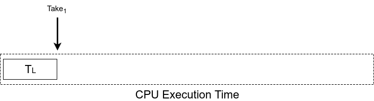
Figure 1. Low priority task is currently running and takes a semaphore.
.png)
Figure 2. OS Tick event occurs.
.png)
Figure 3. High priority task is ready to run and selected to run.
.png)
Figure 4. High priority task attempts to take semaphore and blocks.
.png)
Figure 5. Since high priority task is blocked, the next ready task that can run is the low priority task. The OS tick event occurs.
.png)
Figure 6. The OS tick event occurs, a middle priority task, that never sleeps is ready to run, it begins to run, high priority task is blocked on semaphore and low priority task is blocked by the middle priority task. This is priority inversion, where a medium priority task is running over a higher priority task.
Priority Inheritance using Mutex
Priority inheritance is the means of preventing priority inversion.
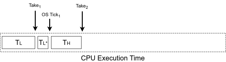
Figure 7. Moving a bit further, the high priority task attempts to take the Mutex
.png)
Figure 8. Low priority task inherates the highest priority of the task that attempts to take the mutex it posses.
.png)
Figure 9. OS Tick2 occurs, and medium priority task is ready, but the low priority task has inheritated a higher priority, thus it runs above the medium priority task.
.png)
Figure 10. Low priority task gives the mutex, low priority task de-inheritates its priority, and the high task immediately begins to run. It will run over the medium task.
.png)
Figure 11. At give2 high priority task releases the mutex and sleeps. Some time elapses, and then the medium task begins to run. No priority inversion occurs in this scenario, the RTOS rule of highest priority runs first is held.
Design Pattern
The design pattern for a mutex should be exclusively used as a protection token. Mutexes can be used in place of as semaphores but the addition work of priority inheritance will cause this approach to take longer and thus be less efficient than a semaphore.
#include "FreeRTOS.h"
#include "semphr.h"

// In main(), initialize your Mutex:
SemaphoreHandle_t spi_bus_mutex = xSemaphoreCreateMutex();

void task_one()
{
    while(1) {
        if(xSemaphoreTake(spi_bus_mutex, 1000)) {
            // Use Guarded Resource

            // Give Semaphore back:
            xSemaphoreGive(spi_bus_mutex);
        }
    }
}
void task_two()
{
    while(1) {
        if(xSemaphoreTake(spi_bus_mutex, 1000)) {
            // Use Guarded Resource

            // Give Semaphore back:
            xSemaphoreGive(spi_bus_mutex);
        }
    }
}
Other notes
Good APIs actually have protection such that the mutex cannot be given accidentally.
Structured Bit-fields Register Mapping
Please Review the Following
- Structures in C: http://www.cplusplus.com/doc/tutorial/structures/
- Unions in C: http://www.cplusplus.com/doc/tutorial/other_data_types/
Register Structure Mapping
Lets observe the status register for the ADXL362 accelerometer. The choice of this device is arbitrary.

Figure 1. ADXL362 Status Register
Normally, and more portably, to store information about the awake bit, you would do the following:
/* Get byte from accelerometer */
uint8_t status = getStatusByte();
/* Store 6th bit using a shift and mask */
bool awake = ((status >> 6) & 0b1);
// You can also do this (to guarantee the result to be true or false only, rather than 0 or (1 << 6) which is 64
bool awake = (status & (1 << 6)) ? true : false;
bool awake = !!(status & (1 << 6));

/* Now use the stored awake boolean */
if(awake)
{
	doAThing();
}
The above is fine, but it would be great to do this in a more elegant fashion. For example, the following:
/* Get a byte and cast it to our adlx_t structure */
adlx_t status = (adlx_t)getStatusByte();
/* Now retrieve the awake bit using the following syntax */
if(status.awake)
{
	doAThing();
}
To do something like this, you can define the adlx_t structure in the following way:
typedef struct __attribute__((packed))
{
	uint8_t data_ready: 1;
	uint8_t fifo_ready: 1;
	uint8_t fifo_warning: 1;
	uint8_t fifo_overrun: 1;
	uint8_t activity: 1;
	uint8_t : 1; /* Un-named padding, since I don't care about the inactivity signal */
	uint8_t awake: 1;
	uint8_t error: 1;
} adlx_t;
The colon specifies the start of a bit field. The number after the colon is the length in bits that label will take up. The __attribute__((packed)) is a necessary compiler directive, specific to GCC which tells the compiler to make sure that the structure is packed together in the way that it is shown. It also tells the compiler to not rearrange it or expand it in order to make it more efficient to work with by the CPU.
NOTE: that the bit-field example and the shift and mask example are equivalent computationally. One is not necessarily more efficient the other. On one hand, you are writing the mask, in the other, the compiler does this for you.
Using Unions
Lets say we wanted to set the whole structure to zeros or a specific value, we can do this using unions.
typedef union
{
	uint8_t byte;
	struct
	{
		uint8_t data_ready: 1;
		uint8_t fifo_ready: 1;
		uint8_t fifo_warning: 1;
		uint8_t fifo_overrun: 1;
		uint8_t activity: 1;
		uint8_t inactivity: 1;
		uint8_t awake: 1;
		uint8_t error: 1;
	} __attribute__((packed));
} adlx_t;
This allows the user to do the following:
/* Declare status variable */
adlx_t status;
/* Set whole bit field through the byte member */
status.byte = getStatusByte();

/* Use awake bit */
if (status.awake)
{
	doSomething();
}

/* Clear bit field */
status.byte = 0;
What about large data structures? For example, the ID3v1 metadata structure for MP3 files. This datastructure contains title name, artist and many other bits of information about the song to be played. It contains 128 bytes
| Field | Length | Description |
|---|---|---|
| header | 3 | "TAG" |
| title | 30 | 30 characters of the title |
| artist | 30 | 30 characters of the artist name |
| album | 30 | 30 characters of the album name |
| year | 4 | A four-digit year |
| comment | 28 | The comment. |
| zero-byte | 1 | If a track number is stored, this byte contains a binary 0. |
| track | 1 | The number of the track on the album, or 0. Invalid, if previous byte is not a binary 0. |
| genre | 1 | Index in a list of genres, or 255 |
This is not a bit field, but the same principles stand. This can be turned into a structure as well:
typedef union
{
	uint8_t buffer[128];
	struct
	{
		uint8_t header[3];
		uint8_t title[30];
		uint8_t artist[30];
		uint8_t album[30];
		uint8_t year[4];
		uint8_t comment[28];
		uint8_t zero;
		uint8_t track;
		uint8_t genre;
	} __attribute__((packed));
} ID3v1_t;
Now, it would take up 128 bytes of memory in to create one of these structures and we want to be conservative. To use use the structure properties, and reduce space usage you can utilize pointers and casting.
ID3v1_t mp3;

/* Some function to get the ID3v1 data */
dumpMP3DataIntoBuffer(&mp3.buffer[0]);

/* Compare string TAG with header member */
printf(" Title: %.30s\n", mp3.title);
printf("Artist: %.30s\n", mp3.artist);
Using Macros
Using some casting techniques and macros you can do something like the following:
#define ADLX(reg) (*((adlx_t*)(®)))
uint8_t status = getStatusByte();
if (ADLX(status).awake)
{
doAThing();
}Dangers of Using Bit-fields
The above example that does not use bit-fields is quite portable, but bit-field mapping can be problematic depending on these factors
-
Endianess of your system: If a bit-field of a status register is little-endian and your processor is big-endian, the bits will be flipped.
- This link explains this further: http://opensourceforu.com/2015/03/be-cautious-while-using-bit-fields-for-programming/
- Structure of your struct: in gcc, using __attribute__((packed)) is very important, because the compiler may attempt to optimize that structure for speed, by expanding the members of the struct into 32-bits, or it may reorder the members and bit to make easier to do operations on. In these cases, the mapping will no longer work. This is something to consider when using this. This also typically depends on the compiler options for compiling.
- Mixing bit fields and members: See the link below on some issues that occurred when you mix bit-fields with variables.
Lab: SPI Flash Interface
The objective is to learn how to create a thread-safe driver for Synchronous Serial Port and to communicate with an external SPI Flash device.
This lab will utilize:
- SPI driver (LPC user manual calls SPI as SSP)
- Code interface for the SPI flash
- Basic knowledge of data structures
- Mutex strategy to access the SPI flash safely across multiple tasks (or threads)
- Logic Analyzer capture
Important Reminders
- Do not forget to select the PIN functions such that the peripheral can control SCK, MOSI, and MISO pins
- These should be IOCON registers of LPC40xx
- You will not use the SSEL pin of the SPI driver
- The pin that shows SSEL is actually purposed as a GPIO to select the external SPI flash memory
- SSEL pin is meant for the purpose of your microcontroller acting as a SLAVE but since you are trying to be the master, this SSEL pin does not apply to you. It is instead re-purposed as a GPIO for your SPI flash memory.
- Please read this great article also
Assignment
Part 0: SPI Driver

Preparation:
- Before you start the assignment, please read Chapter 21: SSP in your LPC User manual (
UM10562.pdf). You can skip the sections related to interrupts or the DMA.- From LPC User manual to understand the different registers involved in writing a SSP2 driver
- Refer table 84 from LPC User manual for pin configuration
- From the schematics pdf(
Schematics-RevE.2.pdf), identify the pin numbers connected to flash memory and make a note of it because you will be needing them for pin function configuration - Read the external SPI flash datasheet (
DS-AT25DN256_039.pdf) or (DS-AT25SF041_044) depends on the board.
Implement ssp2_lab.h and ssp2_lab.c
Note that there is already an ssp2.h in your sample project, but you will re-write this driver. Refrain from peeking the existing driver because you will have to re-write more complex drivers during your exams without any reference code. If you get a compiler error about 'duplicate symbol' then please re-name your SSP functions accordingly because this compiler error may be stating that there is existing function with the same name in the SPI driver in another file.
#include <stdint.h>

void ssp2__init(uint32_t max_clock_mhz) {
  // Refer to LPC User manual and setup the register bits correctly
  // a) Power on Peripheral
  // b) Setup control registers CR0 and CR1
  // c) Setup prescalar register to be <= max_clock_mhz
}

uint8_t ssp2__exchange_byte(uint8_t data_out) {
  // Configure the Data register(DR) to send and receive data by checking the SPI peripheral status register
}
Part 1: SPI Flash Interface
Get the code below to work and validate that you are able to read SPI flash memory's manufacture id and compare it with the SPI flash datasheet to ensure that this is correct.
#include "FreeRTOS.h"
#include "task.h"

#include "ssp2_lab.h"

// TODO: Implement Adesto flash memory CS signal as a GPIO driver
void adesto_cs(void);
void adesto_ds(void);

// TODO: Study the Adesto flash 'Manufacturer and Device ID' section
typedef struct {
  uint8_t manufacturer_id;
  uint8_t device_id_1;
  uint8_t device_id_2;
  uint8_t extended_device_id;
} adesto_flash_id_s;

// TODO: Implement the code to read Adesto flash memory signature
// TODO: Create struct of type 'adesto_flash_id_s' and return it
adesto_flash_id_s adesto_read_signature(void) {
  //adesto_flash_id_s data = { 0 };

  adesto_cs();
  {
    // Send opcode and read bytes
    // TODO: Populate members of the 'adesto_flash_id_s' struct
  }
  adesto_ds();

  //return data;
}

void spi_task(void *p) {
  const uint32_t spi_clock_mhz = 24;
  ssp2__init(spi_clock_mhz);

  // From the LPC schematics pdf, find the pin numbers connected to flash memory
  // Read table 84 from LPC User Manual and configure PIN functions for SPI2 pins
  // You can use gpio__construct_with_function() API from gpio.h
  //
  // Note: Configure only SCK2, MOSI2, MISO2.
  // CS will be a GPIO output pin(configure and setup direction)
  todo_configure_your_ssp2_pin_functions();

  while (1) {
    adesto_flash_id_s id = adesto_read_signature();
    // TODO: printf the members of the 'adesto_flash_id_s' struct

    vTaskDelay(500);
  }
}

void main(void) {
  xTaskCreate(spi_task, ...);
  vTaskStartScheduler();
}
Part 2: SPI Flash Interface with a Mutex
- Read the article in this link to understand how a mutex is created and used in a task
- Purposely comment out the task creation of the task from Part 1:
xTaskCreate(spi_task,...) - Study the code below which will attempt to read Adesto flash manufacturer ID in two tasks simultaneously
- Run the following code, and confirm that it fails
- Be sure to initialize your SPI, and CS GPIO as needed
#include "FreeRTOS.h"
#include "task.h"

#include "ssp2_lab.h"

void spi_id_verification_task(void *p) {
  while (1) {
    const adesto_flash_id_s id = ssp2__adesto_read_signature();

    // When we read a manufacturer ID we do not expect, we will kill this task
    if (0x1F != id.manufacturer_id) {
      fprintf(stderr, "Manufacturer ID read failure\n");
      vTaskSuspend(NULL); // Kill this task
    }
  }
}

void main(void) {
  // TODO: Initialize your SPI, its pins, Adesto flash CS GPIO etc...

  // Create two tasks that will continously read signature
  xTaskCreate(spi_id_verification_task, ...);
  xTaskCreate(spi_id_verification_task, ...);

  vTaskStartScheduler();
}
After you confirm that there is a failure while two tasks try to use the SPI bus, resolve this by using a Mutex:
- Protect your
ssp2__adesto_read_signature()a function such that two tasks will not be able to run this function at the same time. - If implemented correctly, you will not see the error
printf
Part 3: Extra Credit
Develop functionality to be able to read and write a "page" of the SPI flash memory. Here is a sample code that you can reference to send a uint32_t address to the SPI flash with MSB first.
#include <stdint.h>

/**
 * Adesto flash asks to send 24-bit address
 * We can use our usual uint32_t to store the address
 * and then transmit this address over the SPI driver
 * one byte at a time
 */
void adesto_flash_send_address(uint32_t address) {
  (void) ssp2__exchange_byte((address >> 16) & 0xFF);
  (void) ssp2__exchange_byte((address >>  8) & 0xFF);
  (void) ssp2__exchange_byte((address >>  0) & 0xFF);
}
Conclusion
Logic Analyzer Hints
Saleae logic analyzer is a high quality USB analyzer, although you can find many copy cats as well. After you install the software, do the following:
- Hook up SCK, MOSI, and MISO to particular colors, and configure these colors by selecting the SPI bus in logic analyzer software (on windows for example)
- Setup a trigger
- You have to setup a "trigger" which will trigger the logic analyzer data capture
- The CS signal transitioning from HIGH to LOW is the right choice, however, the CS signal may not be broken out on a pin header
- To provide a trigger, what you can do is that you can SET and RESET two GPIO pins simultaneously. One pin would be the real pin going to Adesto flash, and the second one is an arbitrary pin which is available on your SJ2 pin header that you can connect to the logic analyzer as a trigger
Saleae logic analyzers are fast, but some others are not as fast. What this means is that you should ensure that your speed of the analyzer is FASTER than the SPI speed that you set. If for example your logic analyzer is only 6Mhz, then you should set your SPI speed slower than 6Mhz otherwise it will not capture the data correctly.
Requirements and what to turn in
- Include all the code you developed in this lab
- Turn in the screenshots of terminal output
- Include Manufacturer ID
- Logic Analyzer Screenshots
- This lab requires logic analyzer screenshots. Visit SCE, CmpE294, to borrow Saleae logic analyzer
- Connect your pins to the SSP2 MISO, MOSI, SCK and CS signals to the logic analyzer, and select the option in Saleae program to decode SPI frames
- In your turned in Canvas artifacts, include the waveform of SPI retrieving manufacture ID
Lab: SPI bus contention with SD Card
Overview
- Build your own SPI2 driver
- You will initialize your pins
- You will initialize SPI2 peripheral
- Using existing driver, validate the micro-SD card API to get "sector count"
- The sector count gives you information about the total capacity of the SD card
- Replace the SD card to use your own functions
- Validate if you are able to read the data correctly
- Produce a deliberate race condition while two tasks are reading the sector count
- Use a mutex to solve the race condition
Part 0: Micro-SD Card
In this part, you will familiarize yourself with the low level functions that use the SPI bus to communicate with the (micro) SD card. You will use pre-existing SPI driver in this part just to prove that you are able to communicate with the SD card.
Inspect the following:
- Do a code walkthrough of the
sd_card.h - Study the
sd_card__ioctl()function - Ensure that your micro-SD card is formatted with FAT32
Insert the SD card, and obtain and print the following information in an RTOS task:
- Sector count
- Sector size
- Block size
- Card Identification Number (
MMC_GET_CID)
Part 1: SPI Driver
In this part, write your own SPI driver. Note that, there is already the ssp2.h driver, but the purpose of this exercise is to get practice writing a driver on your own because you will be tested (and quizzed) on this.
 void spi2_power_on(void) {
  // TODO: Enable PCONP bit: LPC_SC->PCONP
}

void spi_init(void) {
  // TODO:
}

char spi_exchange_byte(char byte_out) {
  // TODO: Ask SPI peripheral to start to send the data
  // TODO: Wait for transfer to complete
  // TODO: Capture the data
}
Part 2: Validate your SPI Driver using Part 0
In this part, you will swap out the existing SPI driver with your hand written driver.
// Open : sd_card_defiines.h

// Swap out existing driver implementation with your own:
#define SD_CARD__TRANSMIT_BYTE(byte)    YOUR_ssp2__exchange_byte(byte)
#define SD_CARD__RECEIVE_BYTE()         YOUR_ssp2__exchange_byte(0xff)
Ensure that you can still read the data from the SD card using your own SPI functions. Note that going through the exercise to develop your own driver is critical, and you don't want to merely copy the existing implementation. Hence, please make sure that you are able to write a driver by reading the datasheet alone.
Part 3: Create race condition
In this part, we will re-use the code from Part-0, but attempt to do so in multiple tasks simultaneously.
static void sd_card_read_task(void *p) {
  while (1) {
    // TODO: Read SD card parameters
    // Print them out
    // TODO: Add a small amount of sleep
  }
}

void main(void) {
  // Create two reader tasks that will attempt to read the SPI bus at the same time
  xTaskCreate(sd_card_read_task, "sd", 4000/sizeof(void*), NULL, PRIORITY_LOW, NULL);
  xTaskCreate(sd_card_read_task, "sd", 4000/sizeof(void*), NULL, PRIORITY_LOW, NULL);

  vTaskStartScheduler();
}
Part 4: Mutex to the rescue
In this part, solve the race condition issue by using the SD card. Simply surround the critical section of the code that you don't want to access in multiple tasks. See the following pages for reference:
For bonus points, can you figure out how the File I/O is race condition free that uses the SD card APIs? For example, try reading or writing files simultaneously in multiple tasks and you will notice that the code works robustly. Can you figure out the mutex that the File I/O APIs use to solve this problem?