SJSU - Embedded Drivers & RTOS
This book covers material that will be utilized in CMPE 146 and CMPE 244
- Getting Started with Preet's Classes
- Project: MP3 Player (CmpE146)
- Project: Video Game (CmpE244)
- SJ2 Board and Software
- Lesson FreeRTOS + LPC40xx
- Lesson GPIO
- Lesson Interrupts
- Lookup Tables
- Binary Semaphores
- Nested Vector Interrupt Controller (NVIC)
- Lab: Interrupts and Binary Semaphores
- Lesson ADC + PWM
- Pin Selection and Pin Mode
- ADC (Analog to Digital Converter)
- PWM (Pulse Width Modulation)
- Lab: ADC + PWM
- Lesson SPI
- SPI (Serial & Peripheral Interface)
- Mutexes
- Structured Bit-fields Register Mapping
- Lab: SPI Flash Interface
- Lab: SPI bus contention with SD Card
- Lesson UART
- Lesson I2C
- Lesson Watch Dogs
- Lesson X
- FreeRTOS X
Getting Started with Preet's Classes
Advise from prior students:
-
I have 8 years experience in the industry and this class is very industry oriented. Pay attention to the code review comments. They're very helpful.
-
Definitely not a beginner's course, so in order to not be overwhelmed, make sure that you have an understanding of c/c++.
-
Try to understand the concepts and do not solve the assignment only for grades, but for knowledge.
-
Know your basics of C and electrical engineering
-
Don't miss class.
-
DO THE LABS. They provide so much essential knowledge and structured understanding of the RTOS concepts
-
Brush up on your c and datasheet reading knowledge
-
Don't procrastinate, This class can get you an interview!!!
-
Start labs early, get comfortable with Git
-
Definitely keep ahead of the homework and start early - the first 6-8 weeks are rough, but things start to connect and the productivity stays the same working through the project even with lesser homework pressure.
Useful Knowledge
Project: MP3 Player (CmpE146)
MP3 Project
Project Summary
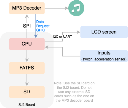
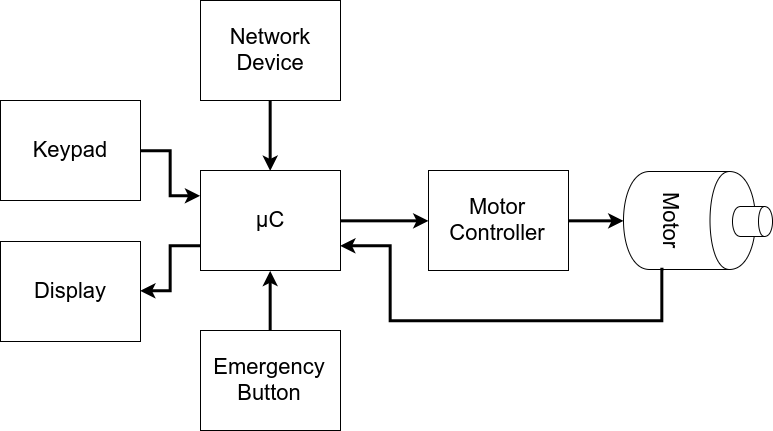
The goal of this project is to create a fully functional MP3 music player using SJOne/SJ2 Microcontroller board as the source for music and control. MP3 files will be present on an SD card. SJOne board reads these files and transfers data to a audio decoding peripheral for generating music. User would be able to use player controls (start/stop/pause) for playing MP3 songs and view the track information on a display.
Block Diagram
Design
Split your project into manageable RTOS tasks. There should be dedicated tasks for:
- Reading an MP3 file
- Playing an MP3 file
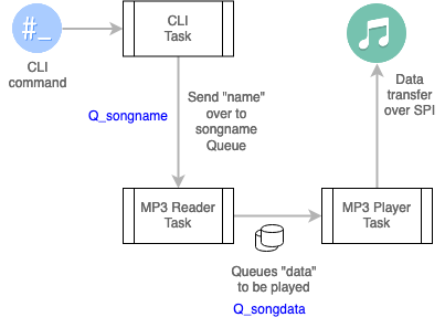
Here is the psuedocode:
typedef char songname_t[16];
QueueHandle_t Q_songname;
QueueHandle_t Q_songdata;
void main(void) {
Q_songname = xQueueCreate(1, sizeof(songname));
Q_songdata = xQueueCreate(1, 512);
}
// Reader tasks receives song-name over Q_songname to start reading it
void mp3_reader_task(void *p) {
songname name;
char bytes_512[512];
while(1) {
xQueueReceive(Q_songname, &name[0], portMAX_DELAY);
printf("Received song to play: %s\n", name);
open_file();
while (!file.end()) {
read_from_file(bytes_512);
xQueueSend(Q_songdata, &bytes_512[0], portMAX_DELAY);
}
close_file();
}
}
// Player task receives song data over Q_songdata to send it to the MP3 decoder
void mp3_player_task(void *p) {
char bytes_512[512];
while (1) {
xQueueReceive(Q_songdata, &bytes_512[0], portMAX_DELAY);
for (int i = 0; i < sizeof(bytes_512); i++) {
while (!mp3_decoder_needs_data()) {
vTaskDelay(1);
}
spi_send_to_mp3_decoder(bytes_512[i]);
}
}
}
// CLI needs access to the QueueHandle_t where you can queue the song name
// One way to do this is to declare 'QueueHandle_t' in main() that is NOT static
// and then extern it here
extern QueueHandle_t Q_songname;
app_cli_status_e cli__mp3_play(app_cli__argument_t argument,
sl_string_t user_input_minus_command_name,
app_cli__print_string_function cli_output) {
// user_input_minus_command_name is actually a 'char *' pointer type
// We tell the Queue to copy 32 bytes of songname from this location
xQueueSend(Q_songname, user_input_minus_command_name, portMAX_DELAY);
printf("Sent %s over to the Q_songname\n", user_input_minus_command_name);
return APP_CLI_STATUS__SUCCESS;
}Project Requirements
Non-Functional Requirements:
- Should be dynamic.
- As in, you should be able to add more songs and play them
- Should be accurate.
- Audio should not sound distorted,
- Audio should not sound slower or faster when running on your system.
- Should be user friendly.
- User should be able to figure out how to use the device without a user manual.
- Product must be packaged in some enclosure. No wires can be vision for the project.
Functional Requirements
- System must use the SJOne/SJ2 on board SD card to read MP3 audio files.
- System must communicate to an external MP3 decoder
- System must allow users to control the MP3 player (You may use the onboard buttons for this)
- User must be able to play and pause of song
- user must be able to select a song
- System must use an external display to show a menu providing the following information:
- Current playing song
- Information about current playing song
- Menu showing how to select a different song
- (Not all of the above need to be shown on the same display)
- System software must separated into tasks. EX: Display task, MP3 Read Task, Controller Task etc...
- System software must be thread safe always.
- System software must use OS structures and primitives where applicable.
- System software may only utilize 50% or less CPU
- You must have an LCD screen for "diagnostics" where you print the CPU utilization and update it at least every 1 second
Prohibited Actions:
- System MAY NOT use an external SD card reader embedded into MP3 device. YOU MAY use an external SD card reader if your SD card reader is broken
- You must interface to external LCD screen (not the on-board LCD screen)
- On-board screen is too small
- The goal is to interface to external components (practice with HW design)
- Use of any external libraries (specifically Arduino) that drive the hardware you intent to use. You must make the drivers from scratch for every part you make.
Permitted Action:
- You may use the internal buttons for controlling the MP3 player.
- You may use the 7-segment display and LEDs above buttons for debugging but not as the main menu.
Song list code module
Collect MP3 song list from the SD card
Reference Articles
Get a list of MP3 files (naive way)
The objective of this code is to get a list of *.mp3 files at the root directory of your SD card.
#include "ff.h"
void print_list_of_mp3_songs(void) {
FRESULT result;
FILINFO file_info;
const char *root_path = "/";
DIR dir;
result = f_opendir(&dir, root_path);
if (result == FR_OK) {
while (1) {
result = f_readdir(&dir, &file_info);
const bool item_name_is_empty = (file_info.fname[0] == 0);
if ((result != FR_OK) || item_name_is_empty) {
break; /* Break on error or end of dir */
}
const bool is_directory = (file_info.fattrib & AM_DIR);
if (is_directory) {
/* Skip nested directories, only focus on MP3 songs at the root */
} else { /* It is a file. */
printf("Filename: %s\n", file_info.fname);
}
}
f_closedir(&dir);
}
}
Get list of MP3 songs
Here is a better way to design code such that a dedicated code module will obtain song-list for you:
// @file: song_list.h
#pragma once
#include <stddef.h> // size_t
typedef char song_memory_t[128];
/* Do not declare variables in a header file */
#if 0
static song_memory_t list_of_songs[32];
static size_t number_of_songs;
#endif
void song_list__populate(void);
size_t song_list__get_item_count(void);
const char *song_list__get_name_for_item(size_t item_number);
#include <string.h>
#include "song_list.h"
#include "ff.h"
static song_memory_t list_of_songs[32];
static size_t number_of_songs;
static void song_list__handle_filename(const char *filename) {
// This will not work for cases like "file.mp3.zip"
if (NULL != strstr(filename, ".mp3")) {
// printf("Filename: %s\n", filename);
// Dangerous function: If filename is > 128 chars, then it will copy extra bytes leading to memory corruption
// strcpy(list_of_songs[number_of_songs], filename);
// Better: But strncpy() does not guarantee to copy null char if max length encountered
// So we can manually subtract 1 to reserve as NULL char
strncpy(list_of_songs[number_of_songs], filename, sizeof(song_memory_t) - 1);
// Best: Compensates for the null, so if 128 char filename, then it copies 127 chars, AND the NULL char
// snprintf(list_of_songs[number_of_songs], sizeof(song_memory_t), "%.149s", filename);
++number_of_songs;
// or
// number_of_songs++;
}
}
void song_list__populate(void) {
FRESULT res;
static FILINFO file_info;
const char *root_path = "/";
DIR dir;
res = f_opendir(&dir, root_path);
if (res == FR_OK) {
for (;;) {
res = f_readdir(&dir, &file_info); /* Read a directory item */
if (res != FR_OK || file_info.fname[0] == 0) {
break; /* Break on error or end of dir */
}
if (file_info.fattrib & AM_DIR) {
/* Skip nested directories, only focus on MP3 songs at the root */
} else { /* It is a file. */
song_list__handle_filename(file_info.fname);
}
}
f_closedir(&dir);
}
}
size_t song_list__get_item_count(void) { return number_of_songs; }
const char *song_list__get_name_for_item(size_t item_number) {
const char *return_pointer = "";
if (item_number >= number_of_songs) {
return_pointer = "";
} else {
return_pointer = list_of_songs[item_number];
}
return return_pointer;
}int main(void) {
song_list__populate();
for (size_t song_number = 0; song_number < song_list__get_item_count(); song_number++) {
printf("Song %2d: %s\n", (1 + song_number), song_list__get_name_for_item(song_number));
}
}Project: Video Game (CmpE244)
LED Matrix Driver
Introduction
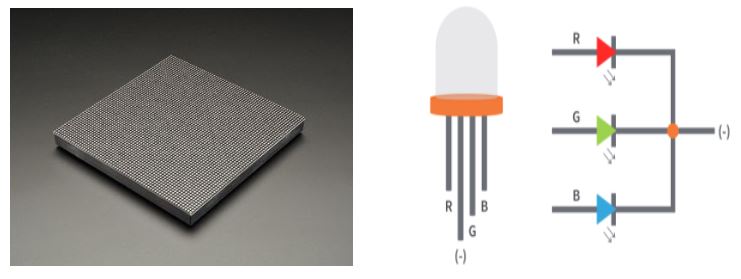
An LED matrix is different from most panel displays. The LEDs are standard tri-color RGB LEDs. Each color on each LED is driven by one bit of a 3-bit shift register. These shift registers are then connected to one another with one shift registers output to the next registers input in a process known as a Daisy Chaining.
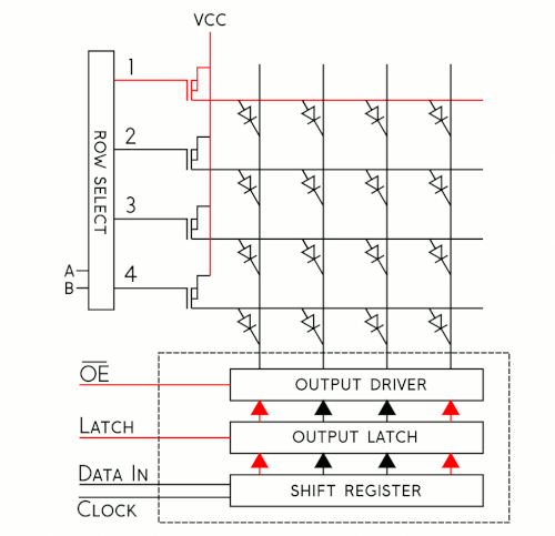
Figure1. 4 x 4 LED Matrix Latching Data (Provided by Sparkfun)
In the above figure, an example 4 by 4 matrix is used to show the steps of how data is clocked into the board.
- Starting from the first Row, select what color you want for each LED in the Row
- Now Enter the 3 bits of data that creates that color into DataIn and Clock it into the Shift Register. Repeat this process for every LED in the Row
- Pull both Output Enable And Latch High, which disables your display and moves the data within the shift registers to the output Latch respectively.
- Using Address Lines A and B, select the next row you want to alter
- Set the Latch and Output Enable Low, which enables your display and lets you write Data to the next Row.
With this method of driving your matrix keep in mind that:
- If you want to alter one LED within a row, you need to enter the data for every LED before it in the row. If you want to clock the color data for say the 27th LED in a particular row you also need to include the data of the 26 other LEDs behind it as well. It is like climbing a ladder, you cannot just start climbing at the tenth rung, you have to climb the first nine first.
- Due to the nature of the shift register their is no native PWM support although you can achieve more colors through Binary code Modulation and Image Planes
LED matrix Parameters & Pins
Most of you will end up buying from SparkFun and Adafruit and most likely pick matrices with the following dimensions with the following scan rates.
- 32 by 32 with a scan rate of 1:16
- 32 by 64 with a scan rate of 1:16
- 64 by 64 with a scan rate of 1:32
It's fairly obvious that the bigger the matrix the more resolution you have to work with for your game. However you will also need to potentially provide more current for your board. A 5V 4A power supply is usually preferred in the absolute worst case where all LEDs are lit up at once, but for many of you a 5V 3A power supply will be sufficient. The pins for the board will typically be as follows:
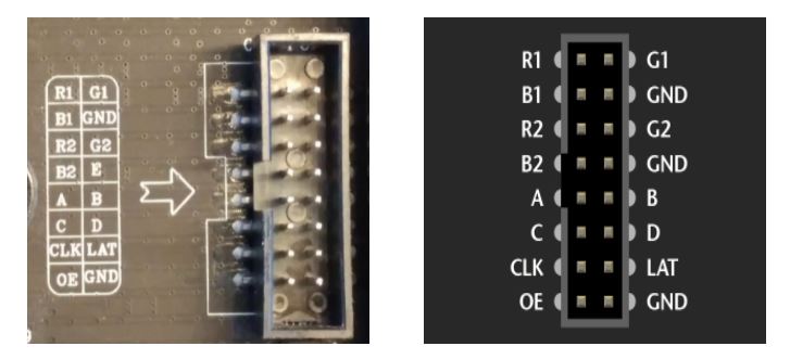
Figure 2. To the Left, a 64 by 64 Matrix Input Pin, To the Right a 32 by 32 or 32 by 64 version
|
Matrix LED pins |
Function |
|
R1 |
High R data |
|
G1 |
High G data |
|
B1 |
High B data |
|
R2 |
Low R data |
|
G2 |
Low G data |
|
B2 |
Low B data |
|
A |
Row select A |
|
B |
Row select B |
|
C |
Row select C |
|
D |
Row select D |
|
E (Potentially Another GND ) |
Row select E (Or GND) |
|
CLK |
Clock signal. |
|
OE |
Active Low Output Enables LED panel Cascade |
|
LAT |
Latch denotes the end of data. |
|
GND |
GND |
Taking a 64 by 64 matrix as an example you will note that there are only 5 address pins A,B,C,D, and E which would only let you access 25 = 32 rows so how would you write data to the other 32?
The scan rates listed above are technical specs for a Matrix board that simply describes how many LEDs are lit up on it at a time. For example a 64 by 64 matrix has 4096 LEDs total. With a scan rate of 1:32 that means that at any given time 4096/32 = 128 LEDs are lit up at a time. Notice that number is exactly two rows of your example 64 by 64 matrix. The matrix displays the data you supplied to the rows via a scanning method starting from the first row of the top half of the board and the first row of the second half of the board. This method divides the 64 by 64 matrix into two 32 row chunks that can be easily addressed with 5 address pins, but how do you decide WHICH of the chunks you talk to?
Notice that there are 6 data pins R1,G1,B1,R2,G2 and B2. As you expect, the RGB1 pins will provide the data to the row you are selecting in the top half of the board and the RGB2 pins will provide the data to the row you are selecting in the bottom half of the board. This scanning is visualized below.

Figure 3. Scan Rate visualized (Provided by Sparkfun)
So if only two rows are being displayed at a time, how can it appear like all the LEDs are lit up? LED matrices use the same persistence of vision explored in your PWM lab to display full images by “scanning” your image at a high enough frequency that your eye can’t keep up with. Most of your matrices should have included a refresh frequency as part of the technical specs. This frequency is the target your Sjtwo board must provide to the LED board to display your image. For this 64 by 64 example, 400Hz is the refresh frequency so your board would need to provide a clock frequency at or above this number. If the frequency is low enough you will be able to see the pattern above. The clock speed you provide to your board will be the speed your game runs at. Most modern day games run at 30 frames per second (fps) or 60 fps which translated to frequency is 30 Hz and 60Hz respectively. Your matrices will most likely be operating at much higher hertz so take this into account when designing animation and game logic that relies on time
We can finally summarize how our LED driver must be written
- Starting from the first Row of you matrix, Select what color you want to clock in to the LED
- Determine if that LED is in the upper or lower portion of your LED and clock that data in using either the RGB1 pins or RGB2 pins
- Set the bits and Clock them in and repeat this process for all the LEDs in the row
- Once a full row has been entered, disable the Output and set Latch High
- Using A,B,C,D,E pins, specify the next row to write to
- Set Latch back down to low and re-enable the Output
- Repeat this process until your entire Matrix has been written to
led_driver.h
#pragma once
#include <stdio.h>
typedef enum {//Color combinations of a RGB LED, experiment with the values
Black,
Blue,
Green,
Cyan,
Red,
Purple,
Yellow,
White
} color_code;
//Should set up all your matrix Pins
void led_driver__matrixInit(void);
//Should set the color of an LED anywhere on board
void led_driver__setPixel(uint8_t row, uint8_t col, color_code color);
//Should draw out a row on your board
void led_driver__drawRow(uint8_t row);
//Should draw the whole LED matrix
void led_driver__drawBoard(void);SJ2 Board and Software
SJ2 Development Environment
There are two major components of the development environment:
- Compile a program for the ARM processor (such as the SJ2 board)
- Compile a program for your host machine (your laptop)
Get started with the development environment by either:
- Download and install Git and then clone the SJ2-C repository
- Go to the SJ2-C repository and download the zip file
Compile the SJ2 project
Most of the documentation related to the ARM compiler is captured in a few README files that you can read here. We will not repeat the details here so please read the linked article. You can watch the following video to get started:
Hands-on
After setting up the SJ2-C development environment, try the following:
- Compile the FreeRTOS sample project (
lpc40xx_freertos) - Load it onto the processor
- Modify the program (maybe printf statement), and load/run it again
- Use a serial terminal program
- Recommend: https://libhal.github.io/web-
serial/
- Recommend: https://libhal.github.io/web-
- Type "help" at the terminal window. Also try "help <command name>"
- Use all of the possible commands, and briefly skim through the code at
handlers_general.cto get an idea of how the code works for each command.
Troubleshooting
Computer cannot recognize the SJ2 development board.
- This error normally happens because of missing Silicon Lab driver.
- Solution: check the install folder inside the development packet (...sjtwo-c-master\installs\drivers). Please Install the driver, then start the computer and try to connect the device again.
"No such file or directory " after running Scons command.
- Please check, if the directory to the development folder has a name, which contain white space.
- Solution: Don’t use directory with spaces.
Cannot recognize the command Scons.
- This error normally happens when Scons is not installed, there are corruption during the installation Scons packet. Sometimes, you need to upgrade the pip to latest version in order to install Scons
- Solution: Please check the pip version and upgrade the pip to latest version, then reinstall the Scons if necessary. After installation, restart the computer and try the Scons command again.
"Sh 1 : python : not found" after running Scons command
- It might appear when you have a multiple python versions, or you already had a python with different management packet (For example, python is installed in your machine through Anaconda, etc ). As the result, the python path might not setup correctly.
-
Solution: Please check out these two article for your best option:
- Window users: https://datatofish.com/add-python-to-windows-path/
- Linux users: https://www.tutorialspoint.com/python3/python_environment.htm
- To make it simple, You can also uninstall the python environment, and download the latest python version here then reinstall it again ( check in Add Python x.y to PATH at the beginning of the installing option )
Python3 is present, and "python" is not available (such as new Mac OS)
Add the following lines to you ~/.zshrc
alias python=python3
alias pip=pip3
export PATH=$PATH:"$(python3 -m site --user-base)/bin"VMs are not recommended
- While it is possible to pass the serial (COM) port to the VM, it can be really tricky.
- Unless you have prior experience with serial port passthrough, using VMs for this class is not recommended.
- If you are on Windows and want to use Linux, use WSL1 instead of WSL2 or VMs.
Compile x86 project
x86 stands for instruction set for your laptop, which means that the project can be compiled and run on your machine without having to compile, load, and run it on your hex project. Being able to compile a project for your x86 host machine also provides the platform for being able to run unit-tests.
Youtube: x86 FreeRTOS Simulator
SJ2 Board Startup
- The real boot location is actually at
entry_point.c - Initial values of RAM are copied from Flash memory's
*data section- See
startup__initialize_ram()atstartup.c
- See
- ARM core's floating point unit, and interrupts are initialized
- Clock and a timer API is initialized
- Peripherals and sensors are initialized
- Finally, call to
main()is made
Unit-Test Framework
TODO
Extras!
The development environment contains built-in code formatting tool. Each time you compile, it will first reformat the source code according to preset Google coding format.
SJ2 Board
SJ2 board has lots of in-built sensors and a 128*64 OLED. It has 96kb of RAM and 120MHZ CPU.
.png)
Board Layout

Board Reset and Boot System
Normally, the NMI pin is not asserted, and when the board is powered on, it will boot straight to your application space which is where you flashed your program.
When the NMI pin is asserted (through the RTS signal of the USB to the serial port), and Reset is toggled, then the board will boot to a separate 8KB flash memory where NXP wrote their own bootloader. This program communicates with flash.py script to load your program to the application memory space.

SJ2 Board Pins
1. UART Pin Mapping for SJ-2 Board
| SJ2 UART's | TXD | RXD | Multiplexed |
| UART 0 | P0.2 | P0.3 | Bootloader, Serial Debug Output |
| P0.0 | P0.1 | CAN1,I2C1 | |
| UART 1 | P0.15 | P0.16 | SSP0 |
| P2.0 | P2.1 | PWM1 | |
| UART 2 | P0.10 | P0.11 | I2C2 |
| P2.8 | P2.9 | Wi-Fi | |
| UART 3 | P0.0 | P0.1 | CAN1,I2C1 |
| P0.25 | P0.26 | ADCx | |
| P4.28 | P4.29 | Wi-Fi | |
| UART 4 | P0.22 | P2.9 | |
| P1.29 | P2.9 |
2. SSP/SPI Pin Mapping for SJ-2 Board
| SJ2 SPI's | SCK | MISO | MOSI |
| SSP0 | P0.15 | P0.17 | P0.18 |
| P1.20 | P1.23 | P1.24 | |
| SSP1 | P0.7 | P0.8 | P0.9 |
| SSP2 | P1.19 | P1.18 | P1.22 |
| P1.31 | P1.18 | P1.22 |
3. I2C Pin Mapping for SJ-2 Board
| SJ2 I2C's | SDA | SCL | Multiplexed |
| I2C 0 | P1.30 | P1.31 | ADCx |
| I2C 1 | P0.0 | P0.1 | UART0, UART3, CAN1 |
| I2C 2 | P0.10 | P0.11 | UART2 |
| P1.15 | P4.29 |
4. CAN Pin Mapping for SJ-2 Board
| SJ2 CAN's | RD | TD | Multiplexed |
| CAN1 | P0.0 | P0.1 | UART0, I2C1, UART3 |
| P0.0 | P0.22 | ||
| CAN2 | P2.7 | P2.8 |
Pin functionality Selection
A pin's functionality may be selected based on your system design. Here are a few examples:
Select UART3 on P4.28 and P4.29:
#include "gpio.h"
void select_uart3_on_port4(void) {
// Reference "Table 84" at "LPC408x_7x User Manual.pdf"
gpio__construct_with_function(GPIO__PORT_4, 28, GPIO__FUNCTION_2); // P4.28 as TXD3
gpio__construct_with_function(GPIO__PORT_4, 29, GPIO__FUNCTION_2); // P4.29 as RXD3
}A pin function should be set based on one of the 8 possibilities. Here is an example again that sets P0.0 and P0.1 to UART3 (note that the 010 corresponds to GPIO__FUNCTION_2). Of course you can also configureP0.0 and P0.1 as UART0 pins by using GPIO__FUNCTION_4
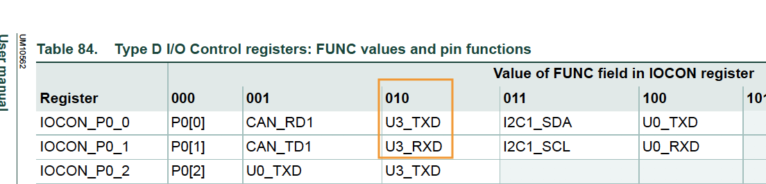
#include "gpio.h"
void select_uart3_on_port0(void) {
gpio__construct_with_function(GPIO__PORT_0, 0, GPIO__FUNCTION_2); // P0.0 as TXD3
gpio__construct_with_function(GPIO__PORT_0, 1, GPIO__FUNCTION_2); // P0.1 as RXD3
}Software Reference
This section focuses on the C software framework, and not the C++ sample project.
CLI Commands
CLI stands for Command Line Interface. The SJ2 C framework includes a way to interact with the board through a CLI command utilizing a CLI task. You can and should add more commands as needed to provide debugging and interaction capability with your board.
You can add your own CLI command by following the steps below:
Step 1: Declare your CLI handler function, the parameters of this function are:
-
app_cli__argument_t: This is not utilized in the SJ2 project, and will beNULL -
sl_string_s: There is a powerful string library type. The string is set to parameters of a CLI command, so if the command name istaskcontroland user inputstaskcontrol suspend led, then the string value will be set tosuspend ledwith the command name removed, seesl_string.hfor more information -
cli_output: This is a function pointer that you should use to output the data back to the CLI
// TODO: Add your CLI handler function declaration to 'cli_handlers.h'
app_cli_status_e cli__your_handler(app_cli__argument_t argument, sl_string_s user_input_minus_command_name,
app_cli__print_string_function cli_output);Step 2: Add your CLI handler
// TODO: Declare your CLI handler struct, and add it at 'sj2_cli.c' inside the sj2_cli__init() function
void sj2_cli__init(void) {
// ...
static app_cli__command_s your_cli_struct = {.command_name = "taskcontrol",
.help_message_for_command = "help message",
.app_cli_handler = cli__your_handler};
// TODO: Add the CLI handler:
app_cli__add_command_handler(&sj2_cli_struct, &your_cli_struct);
}
Step 3: Handle your CLI command
// TODO: Add your CLI handler function definition to 'handlers_general.c' (You can also create a new *.c file)
app_cli_status_e cli__your_handler(app_cli__argument_t argument, sl_string_s user_input_minus_command_name,
app_cli__print_string_function cli_output) {
void *unused_cli_param = NULL;
// sl_string is a powerful string library, and you can utilize the sl_string.h API to parse parameters of a command
// Sample code to output data back to the CLI
sl_string_s s = user_input_minus_command_name; // Re-use a string to save memory
sl_string__printf(s, "Hello back to the CLI\n");
cli_output(unused_cli_param, sl_string__c_str(s));
return APP_CLI_STATUS__SUCCESS;
}
// TODO: Now, when you flash your board, you will see your 'taskcontrol' as a CLI command
Platform Glue
TODO
Newlib and floating point printf and scanf
At the env_arm file, there are a couple of lines you can comment out to save about 18K of flash space. This space is not significant enough when you realize the fact that the LPC controller has 512K of flash ROM space, but it increases a few seconds of programming time each and every time you program.
LINKFLAGS=[
# Use hash sign to comment out the line
# This will disable ability to do printf and scanf of %f (float)
# "-u", "_printf_float",
# "-u", "_scanf_float",
Layout a plan or design of something that is laid out More (Definitions, Synonyms, Translation)
RTOS Trace
Overview
FreeRTOS trace is a third party library developed by Percepio; please check them out here. What you can do is to capture the RTOS trace on the micro-sd card on your SJ2 board which you can later plot out to be able to visualize everything that the RTOS is trying to do.
Install
To get started, you first need to install a Windows trace file viewer. This will open up the trace file saved by the SJ2 board for you to visualize all of the data. You can evaluate the product or get student license for free. Please proceed by visiting the following link:
https://percepio.com/downloadform/
Configure
Now that you have installed the Percepio Trace, it is time to configure the SJ2 software to generate the trace. This is super easy to do:
- First, make sure you have a micro SD card installed on the SJ2 board and formatted in FAT32 format
- Go to
FreeRTOSConfig.hand change this macro#define configENABLE_TRACE_ON_SD_CARD 0
That is pretty much it... you can now compile, and flash the new application and the software will save a file called trace.psf onto the SD card's file system. If you do not see the SD Card blinky light a few times each second, you have likely not loaded the correct application onto the board.
Usage
FreeRTOS Trace can be enabled at FreeRTOS_config.h You can open up an example trace from this Gitlab link which has a pre-existing RTOS trace file generated by the SJ2 board.
There is no general need on how to use the API on the SJ2 board related to the RTOS trace, and the bulk of the "usage" is actually opening up the trace file in Percepio Tracalyzer program. The one thing you could do is "printf" trace data that can be visualized in the trace.
void trace_print(void) {
traceString trace_channel = xTraceRegisterString("trace channel description");
vTracePrintF(trace_channel, "%d: %d", 1, 234);
}
Standart Output
This article provides useful information about how the standard output is handled on the SJ2 platform.
printf
The standard output is connected to UART0. In a bare metal system without the operating system providing means of outputting data to a console, responsibility lies on the developer to connect printf() to your way of outputting data.
In GCC, the function _write() is invoked for all data output related to file handles. On the SJ2 platform, the function is implemented to output data to UART0, which is connected to the USB to serial chip that is interfaced to a computer (such as windows, linux) to see the serial console.
system_calls.c can be referenced to see the full implementation.
int _write(int file_descriptor, const char *ptr, int bytes_to_write) {
// ...
if (rtos_is_running && transmit_queue_enabled && !is_standard_error) {
system_calls__queued_put(ptr, bytes_to_write);
} else {
system_calls__polled_put(ptr, bytes_to_write);
}
return bytes_to_write;
}
fprintf
When fprintf(stderr, "...") is utilized, the system_calls.c does not deposit data to an RTOS queue in which case the data would have been sent out "later" depending on the speed of the UART. The stderr is the key that differentiate polled vs. queued data output.
When the stderr is utilized, this "file handle" triggers the branch statement to output the data using polled UART driver. This means that the CPU cycles will be compromised, and we will waste cycles waiting for data to be sent, so this should not be used in "production code".
printf inside of an ISR
Inside of an interrupt, you never want to "block" using any RTOS API. If we use standard printf(), it may try to enqueue the data to be sent out of the UART0 peripheral, and therefore may crash the system when the UART transmission queue becomes full (as it will then try to sleep on the queue to be not full). Because of this, fprintf(stderr, "...") may be utilized inside of an ISR as it would not enqueue the data or try to "block" through the RTOS API.
In "production intent" code, there should be no printfs inside of an ISR.
Lesson FreeRTOS + LPC40xx
LPC40xx MCU Memory Map
What is a Memory Map
A memory map is a layout of how the memory maps to some set of information. With respect to embedded systems, the memory map we are concerned about maps out where the Flash (ROM), peripherals, interrupt vector table, SRAM, etc are located in address space.
Memory mapped IO
Memory mapped IO is a means of mapping memory address space to devices external (IO) to the CPU, that is not memory.
For example (assuming a 32-bit system)
- Flash could be mapped to address 0x00000000 to 0x00100000 (1 Mbyte range)
- GPIO port could be located at address 0x1000000 (1 byte)
- Interrupt vector table could start from 0xFFFFFFFF and run backwards through the memory space
- SRAM gets the rest of the usable space (provided you have enough SRAM to fill that area)
It all depends on the CPU and the system designed around it.
Port Mapped IO
Port mapped IO uses additional signals from the CPU to qualify which signals are for memory and which are for IO. On Intel products, there is a (~M/IO) pin that is LOW when selecting MEMORY and HIGH when it is selecting IO.
The neat thing about using port mapped IO, is that you don't need to sacrifice memory space for IO, nor do you need to decode all 32-address lines. You can limit yourself to just using 8-bits of address space, which limits you to 256 device addresses, but that may be more than enough for your purposes.

Figure 2. Address Decoding with port map
(http://www.dgtal-sysworld.co.in/2012/04/memory-intercaing-to-8085.html)
LPC40xx memory map
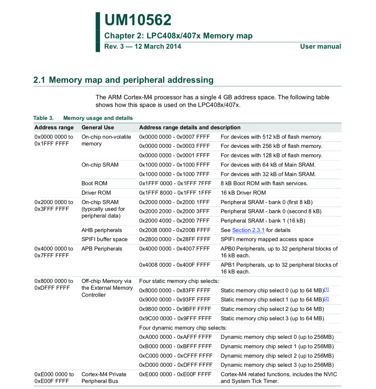
Figure 3. LPC40xx Memory Map
From this you can get an idea of which section of memory space is used for what. This can be found in the UM10562 LPC40xx user manual. If you take a closer look you will see that very little of the address space is actually taken up. With up to 4 billion+ address spaces (because 2^32 is a big number) to use you have a lot of free space to spread out your IO and peripherals.
Reducing the number of lines needed to decode IO
The LPC40xx chips, to reduce bus line count, make all the peripherals 32-bit word aligned. Which means you must grab 4-bytes at a time. You cannot grab a single byte (8-bits) or a half-byte (16-bits) from memory. This eliminates the 2 least significant bits of address space.
Accessing IO using Memory Map in C
Please read the following code snippet. This is runnable on your system now. Just copy and paste it into your main.c file.
/*
The goal of this software is to set the GPIO pin P1.0 to
low then high after some time. Pin P1.0 is connected to an LED.
The address to set the direction for port 1 GPIOs is below:
DIR1 = 0x20098020
The address to set a pin in port 1 is below:
PIN1 = 0x20098034
*/
#include <stdint.h>
volatile uint32_t * const DIR1 = (uint32_t *)(0x20098020);
volatile uint32_t * const PIN1 = (uint32_t *)(0x20098034);
int main(void)
{
// Set 0th bit, setting Pin 0 of Port 1 to an output pin
(*DIR1) |= (1 << 0);
// Set 0th bit, setting Pin 0 of Port 1 to high
(*PIN1) |= (1 << 0);
// Loop for a while (volatile is needed!)
for(volatile uint32_t i = 0; i < 0x01000000; i++);
// Clear 0th bit, setting Pin 0 of Port 1 to low
(*PIN1) &= ~(1 << 0);
// Loop forever
while(1);
return 0;
}volatile keyword tells the compiler not to optimize this variable out, even if it seems useless
const keyword tells the compiler that this variable cannot be modified
Notice "const" placement and how it is placed after the uint32_t *. This is because we want to make sure the pointer address never changes and remains constant, but the value that it references should be modifiable.
Using the LPC40xx.h
The above is nice and it works, but it's a lot of work. You have to go back to the user manual to see which addresses are for what register. There must be some better way!!
Take a look at the lpc40xx.h file, which It is located in the sjtwo-c/projects/lpc40xx_freertos/lpc40xx.h. Here you will find definitions for each peripheral memory address in the system.
Let's say you wanted to port the above code to something a bit more structured:
- Open up "lpc40xx.h"
- Search for "GPIO"
- You will find a struct with the name LPC_GPIO_TypeDef.
- Now search for "LPC_GPIO_TypeDef" with a #define in the same line.
- You will see that LPC_GPIO_TypeDef is a pointer of these structs
#define LPC_GPIO0 ((LPC_GPIO_TypeDef *) LPC_GPIO0_BASE )#define LPC_GPIO1 ((LPC_GPIO_TypeDef *) LPC_GPIO1_BASE )#define LPC_GPIO2 ((LPC_GPIO_TypeDef *) LPC_GPIO2_BASE )#define LPC_GPIO3 ((LPC_GPIO_TypeDef *) LPC_GPIO3_BASE )#define LPC_GPIO4 ((LPC_GPIO_TypeDef *) LPC_GPIO4_BASE )
- We want to use LPC_GPIO1 since that corresponds to the GPIO port 1.
- If you inspect LPC_GPIO_TypeDef, you can see the members that represent register DIR and PIN
- You can now access DIR and PIN registers in the following way:
#include "lpc40xx.h"
int main(void)
{
// Set 0th bit, setting Pin 0 of Port 1 to an output pin
LPC_GPIO1->DIR |= (1 << 0);
//// Set 0th bit, setting Pin 0 of Port 1 to high
LPC_GPIO1->PIN |= (1 << 0);
//// Loop for a while (volatile is needed!)
for(volatile uint32_t i = 0; i < 0x01000000; i++);
//// Clear 0th bit, setting Pin 1.0 to low
LPC_GPIO1->PIN &= ~(1 << 0);
//// Loop forever
while(1);
return 0;
}At first this may get tedious, but once you get more experience, you won't open the lpc40xx.h file very often. This is the preferred way to access registers in this course and in industry.
On occasions, the names of registers in the user manual are not exactly the same in this file.
FreeRTOS & Tasks
Introduction to FreeRTOS
Objective
To introduce what, why, when, and how to use Real Time Operating Systems (RTOS) as well as get you
started using it with the sjtwo-c environment.
I would like to note that this page is mostly an aggregation of information from Wikipedia and the FreeRTOS
Website.
What is an OS?
Operating system (OS) is system software that manages computer hardware and software resources and provides common services for computer programs. - Wikipedia
Operating systems like Linux or Windows
They have services to make communicating with Networking devices and files systems possible without having
to understand how the hardware works. Operating systems may also have a means to multitasking by allow
multiple processes to share the CPU at a time. They may also have means for allowing processes to
communicate together.
What is an RTOS?
An RTOS is an operating system that meant for real time applications. They typically have fewer services such
as the following:
- Parallel Task Scheduler
- Task communication (Queues or Mailboxes)
- Task synchronization (Semaphores)
Why use an RTOS?
You do not need to use an RTOS to write good embedded software. At some point
though, as your application grows in size or complexity, the services of an RTOS might
become beneficial for one or more of the reasons listed below. These are not absolutes,
but opinion. As with everything else, selecting the right tools for the job in hand is an
important first step in any project.
In brief:
- Abstract out timing information
The real time scheduler is effectively a piece of code that allows you to specify the
timing characteristics of your application - permitting greatly simplified, smaller (and
therefore easier to understand) application code.
- Maintainability/Extensibility
Not having the timing information within your code allows for greater maintainability
and extensibility as there will be fewer interdependencies between your software
modules. Changing one module should not effect the temporal behavior of another
module (depending on the prioritization of your tasks). The software will also be less
susceptible to changes in the hardware. For example, code can be written such that it
is temporally unaffected by a change in the processor frequency (within reasonable
limits).
- Modularity
Organizing your application as a set of autonomous tasks permits more effective
modularity. Tasks should be loosely coupled and functionally cohesive units that within
themselves execute in a sequential manner. For example, there will be no need to
break functions up into mini state machines to prevent them taking too long to execute
to completion.
- Cleaner interfaces
Well defined inter task communication interfaces facilitates design and team
development.
- Easier testing (in some cases)
Task interfaces can be exercised without the need to add instrumentation that may
have changed the behavior of the module under test.
- Code reuse
Greater modularity and less module interdependencies facilitates code reuse across
projects. The tasks themselves facilitate code reuse within a project. For an example
of the latter, consider an application that receives connections from a TCP/IP stack -
the same task code can be spawned to handle each connection - one task per
connection.
- Improved efficiency?
Using FreeRTOS permits a task to block on events - be they temporal or external to
the system. This means that no time is wasted polling or checking timers when there
are actually no events that require processing. This can result in huge savings in
processor utilization. Code only executes when it needs to. Counter to that however is
the need to run the RTOS tick and the time taken to switch between tasks. Whether
the saving outweighs the overhead or vice versa is dependent of the application. Most
applications will run some form of tick anyway, so making use of this with a tick hook
function removes any additional overhead.
- Idle time
It is easy to measure the processor loading when using FreeRTOS.org. Whenever the
idle task is running you know that the processor has nothing else to do. The idle task
also provides a very simple and automatic method of placing the processor into a low
power mode.
- Flexible interrupt handling
Deferring the processing triggered by an interrupt to the task level permits the interrupt
handler itself to be very short - and for interrupts to remain enabled while the task level
processing completes. Also, processing at the task level permits flexible prioritization -
more so than might be achievable by using the priority assigned to each peripheral by
the hardware itself (depending on the architecture being used).
- Mixed processing requirements
Simple design patterns can be used to achieve a mix of periodic, continuous and
event driven processing within your application. In addition, hard and soft real time
requirements can be met though the use of interrupt and task prioritisation.
- Easier control over peripherals
Gatekeeper tasks facilitate serialization of access to peripherals - and provide a good
mutual exclusion mechanism.
- Etcetera
- FreeRTOS Website (https://www.freertos.org/FAQWhat.html)
Design Scenario
Building a controllable assembly conveyor belt
Think about the following system. Reasonable complex, right?
Without a scheduler
✓ Small code size.
✓ No reliance on third party source code.
✓ No RTOS RAM, ROM or processing overhead.
✗ Difficult to cater for complex timing requirements.
✗ Does not scale well without a large increase in complexity.
✗ Timing hard to evaluate or maintain due to the inter-dependencies between the different functions.
With a scheduler
✓ Simple, segmented, flexible, maintainable design with few inter-dependencies.
✓ Processor utilization is automatically switched from task to task on a most urgent need basis with no
explicit action required within the application source code.
✓ The event driven structure ensures that no CPU time is wasted polling for events that have not occurred.
Processing is only performed when there is work needing to be done.
* Power consumption can be reduced if the idle task places the processor into power save (sleep) mode,
but may also be wasted as the tick interrupt will sometimes wake the processor unnecessarily.
* The kernel functionality will use processing resources. The extent of this will depend on the chosen
kernel tick frequency.
✗ This solution requires a lot of tasks, each of which require their own stack, and many of which require a
queue on which events can be received. This solution therefore uses a lot of RAM.
✗ Frequent context switching between tasks of the same priority will waste processor cycles.
FreeRTOS Tasks
What is an FreeRTOS Task?
A FreeRTOS task is a function that is added to the FreeRTOS scheduler using the xTaskCreate() API call.
A task will have the following:
- A Priority level
- Memory allocation
- Singular input parameter (optional)
- A Task name
- A Task handler (optional): A data structure that can be used to reference the task later.
A FreeRTOS task declaration and definition looks like the following:
void vTaskCode( void * pvParameters )
{
/* Grab Parameter */
uint32_t c = (uint32_t)(pvParameters);
/* Define Constants Here */
const uint32_t COUNT_INCREMENT = 20;
/* Define Local Variables */
uint32_t counter = 0;
/* Initialization Code */
initTIMER();
/* Code Loop */
while(1)
{
/* Insert Loop Code */
}
/* Only necessary if above loop has a condition */
xTaskDelete(NULL);
}Rules for an RTOS Task
- The highest priority ready tasks ALWAYS runs
- If two or more have equal priority, then they are time sliced
- Low priority tasks only get CPU allocation when:
- All higher priority tasks are sleeping, blocked, or suspended.
- Tasks can sleep in various ways, a few are the following:
- Explicit "task sleep" using API call vTaskDelay();
- Sleeping on a semaphore
- Sleeping on an empty queue (reading)
- Sleeping on a full queue (writing)
Adding a Task to the Scheduler and Starting the Scheduler
The following code example shows how to use xTaskCreate() and how to start the scheduler using vTaskStartScheduler()
int main(int argc, char const *argv[])
{
//// You may need to change this value.
const uint32_t STACK_SIZE = 128;
xReturned = xTaskCreate(
vTaskCode, /* Function that implements the task. */
"NAME", /* Text name for the task. */
STACK_SIZE, /* Stack size in words, not bytes. */
( void * ) 1, /* Parameter passed into the task. */
tskIDLE_PRIORITY,/* Priority at which the task is created. */
&xHandle ); /* Used to pass out the created task's handle. */
/* Start Scheduler */
vTaskStartScheduler();
return 0;
}Task Priorities
High Priority and Low Priority tasks

In the above situation, the high priority task never sleeps, so it is always running. In this situation where the low priority task never gets CPU time, we consider that task to be starved.
Tasks of the same priority
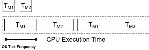
In the above situation, the two tasks have the same priority, thus they share the CPU. The time each task is allowed to run depends on the OS tick frequency. The OS Tick Frequency is the frequency that the FreeRTOS scheduler is called in order to decide which task should run next. The OS Tick is a hardware interrupt that calls the RTOS scheduler. Such a call to the scheduler is called a preemptive context switch.
Context Switching
When the RTOS scheduler switches from one task to another task, this is called a Context Switch.
What needs to be stored for a Context switch to happen
In order for a task, or really any executable, to run, the following need to exist and be accessible and storable:
-
Program Counter (PC)
- This holds the position for which line in your executable the CPU is currently executing.
- Adding to it moves you one more instruction.
- Changing it jumps you to another section of code.
-
Stack Pointer (SP)
- This register holds the current position of the call stack, with regard to the currently executing program. The stack holds information such as local variables for functions, return addresses and [sometimes] function return values.
-
General Purpose Registers
- These registers are to do computation.
-
In ARM:
- R0 - R15
-
In MIPS:
- $v0, $v1
- $a0 - $a3
- $t0 - $t7
- $s0 - $s7
- $t8 - $t9
-
Intel 8086
- AX
- BX
- CX
- DX
- SI
- DI
- BP
-
In ARM:
- These registers are to do computation.
How does Preemptive Context Switch work?
- A hardware timer interrupt or repetitive interrupt is required for this preemptive context switch.
- This is independent of an RTOS.
- Typically, 1ms or 10ms.
- The OS needs hardware capability to have a chance to STOP synchronous software flow and enter the OS “tick” interrupt.
- This is called the "Operating System Kernel Interrupt"
- We will refer to this as the OS Tick ISR (interrupt service routine)
- Timer interrupt calls RTOS Scheduler
- RTOS will store the previous PC, SP, and registers for that task.
- The scheduler picks the highest priority task that is ready to run.
- Scheduler places that task's PC, SP, and registers into the CPU.
- Scheduler interrupt returns, and the newly chosen task runs as if it never stopped.
Tick Rate
Most industrial applications use an RTOS tick rate of 1ms or 10ms (1000Hz, or 100Hz). In the 2000s, probably 100Hz was more common, but as processors got faster, 1000Hz became the norm. One could choose any tick rate, such as 1.5ms per tick, but using such non-standard rates makes API timing non-intuitive, as vTaskDelay(10) would result in sleep time of approximately 15ms. This is yet another reason why 1000Hz is a good tick rate as vTaskDelay(10) would sleep for approximately 10ms, which is intuitive to the developer because the tick times adopt the units of milliseconds.
With a far assumed that the RTOS tick ISR (preemptive scheduling) consumes 200 clock cycles, then on a 20Mhz processor, it would only consume 10uS of overhead per scheduling event. When cooperative scheduling triggers a context switch, it would result in a similar overhead as a "software interrupt" is issued to the CPU to perform the context switch. So this means that each scheduling event has an overhead of 20uS on a 20Mhz processor (assuming 200 clocks for RTOS interrupt). Based on these numbers, here is the overhead ratio of using different tick rates.
| 100Hz | 1000Hz | 10,000Hz (100uS per tick) | |
| Scheduling Overhead per second | 2,000uS | 20,000uS | 200,000uS |
| CPU consumption for RTOS scheduling | 0.2% | 2% | 20% |
Why OS Ticks are 1ms or 1KHz?
1. Shorter Ticks means that there is less time for your code to run. Ex: if OS ticks = 150us instead of 1ms and the context switching takes 100us then you are only left with 50us to complete your task. Hence, RTOS will be only busy with context switching nothing else.
2. Big Ticks such as 4ms, the CPU will remain in the wait state. For example, the context switching takes 100us then you have 3900us to complete your task. However, the task will only take 900us to complete. Then 3000us will be unnecessary overhead on CPU wait time.
Based on the numbers above, 1000Hz is a great balance, while the 10,000Hz tick rate would provide more frequent time slices at the expense of more frequent scheduling overhead.
only and nothing more More (Definitions, Synonyms, Translation)
Lab: FreeRTOS Tasks
Objective
- Load firmware onto the SJ board
- Observe the RTOS round-robin scheduler in effect
- Provide hands-on experience with the UART character output timing
Part 0a. Change UART speed
We will be working with an assumption for this lab, so we will need to change the UART speed. In Visual Studio Code IDE, hit Ctrl+P and open peripherals_init.c. Then modify the UART speed to 38400. After doing so, make sure you open your serial terminal or Telemetry web terminal and change the port speed to also 38400.
static void peripherals_init__uart0_init(void) {
// Do not do any bufferring for standard input otherwise getchar(), scanf() may not work
setvbuf(stdin, 0, _IONBF, 0);
// Note: PIN functions are initialized by board_io__initialize() for P0.2(Tx) and P0.3(Rx)
uart__init(UART__0, clock__get_peripheral_clock_hz(), 38400); // CHANGE FROM 115200 to 38400
// ...
}The peripherals_init__uart0_init() is executed before your main() function. When you are finished with this lab, you can choose to change this back to 115200bps for faster UART speed.
Part 0b. Create Task Skeleton
A task in an RTOS or FreeRTOS is nothing but a forever loop, however unless you sleep the task, it will consume 100% of the CPU. For this part, study existing main.c and create two additional tasks for yourself.
#include "FreeRTOS.h"
#include "task.h"
static void task_one(void * task_parameter);
static void task_two(void * task_parameter);
int main(void) {
// ...
}
static void task_one(void * task_parameter) {
while (true) {
// Read existing main.c regarding when we should use fprintf(stderr...) in place of printf()
// For this lab, we will use fprintf(stderr, ...)
fprintf(stderr, "AAAAAAAAAAAA");
// Sleep for 100ms
vTaskDelay(100);
}
}
static void task_two(void * task_parameter) {
while (true) {
fprintf(stderr, "bbbbbbbbbbbb");
vTaskDelay(100);
}
}Part 1: Create RTOS tasks
- Fill out the
xTaskCreate()method parameters.
- See the FreeRTOS+Tasks document or checkout the FreeRTOS xTaskCreate API website
- Recommended stack size is:4096 / sizeof(void*) - Note that you want to make sure you use
fprintf(stderr, ...)in place ofprintf(...)
-fprintf(stderr, ...)is slower and eats up CPU, but it is useful during debugging
-printf(...)is faster (and efficient), but it queues the data to be "sent later" - Observe the output
- After you flash your program, check the output of the serial console
#include "FreeRTOS.h"
#include "task.h"
static void task_one(void * task_parameter);
static void task_two(void * task_parameter);
int main(void) {
/**
* Observe and explain the following scenarios:
*
* 1) Same Priority: task_one = 1, task_two = 1
* 2) Different Priority: task_one = 2, task_two = 1
* 3) Different Priority: task_one = 1, task_two = 2
*
* Note: Priority levels are defined at FreeRTOSConfig.h
* Higher number = higher priority
*
* Turn in screen shots of what you observed
* as well as an explanation of what you observed
*/
xTaskCreate(task_one, /* Fill in the rest parameters for this task */ );
xTaskCreate(task_two, /* Fill in the rest parameters for this task */ );
/* Start Scheduler - This will not return, and your tasks will start to run their while(1) loop */
vTaskStartScheduler();
return 0;
}
// ...Part 2: Further Observations
Fundamentals to keep in mind:
- FreeRTOS tick rate is configured at 1Khz
- This means that the RTOS preemptive scheduling can occur every 1ms repetitively - Standout output (
printf) is integrated in software to send data to your UART0
- This is the same serial bus that is used to load a new program (or hex file)
- The speed is defaulted to 38400bps, and since there is 10 bits of data used to send 1 byte, we can send as many as 3840 characters per second
Critical thinking questions:
- How come 4(or 3 sometimes) characters are printed from each task? Why not 2 or 5, or 6?
- Alter the priority of one of the tasks, and note down the observations. Note down WHAT you see and WHY.
Hint: You have to relate the speed of the RTOS round-robin scheduler with the speed of the UART to answer the questions above
Part 3. Change the priority levels
Now that you have the code running with identical priority levels, try the following:
- Change the priority of the two tasks
* Same Priority:task_one= 1,task_two= 1
* Different Priority:task_one= 2,task_two= 1
* Different Priority:task_one= 1,task_two= 2 - Take a screenshot of what you see from the console
- Write an explanation of why you think the output came out the way it did using your knowledge about RTOS
Optional: If you have TraceAlyzer program installed, we encourage you to load this file and inspect the trace.
What to turn in:
- Relevant code
- Your observation and explanation
- Snapshot of the output for all scenarios
If your class requires you to turn in the assignment as a Gitlab link, you should:
- Use this article to get started
- Submit a link to Gitlab "Merge Request"
- Be sure to ensure that your Merge Request is only the new code, and not a very large diff
Lesson GPIO
Bitmasking
Bit-masking is a technique to selectively modify individual bits without affecting other bits.
Bit SET
To set a bit, we need to use the OR operator. This is just like an OR logical gate you should've learned in the Digital design course. To set a bit, you would OR a memory with a bit number, and the bit number with which you will OR will end up getting set.
// Assume we want to set Bit#7 of a register called: REG
REG = REG | 0x80;
// Let's set bit#31:
REG = REG | 0x80000000;
// Let's show you the easier way:
// (1 << 31) means 1 gets shifted left 31 times to produce 0x80000000
REG = REG | (1 << 31);
// Simplify further:
REG |= (1 << 31);
// Set Bit#21 and Bit# 23:
REG |= (1 << 21) | (1 << 23);Bit CLEAR
To reset or clear a bit, the logic is similar, but instead of ORing a bit, we will AND a bit. Remember that AND gate clears a bit if you AND it with 0 so we need to use a tilde (~) to come up with the correct logic:
// Assume we want to reset Bit#7 of a register called: REG
REG = REG & 0x7F;
REG = REG & ~(0x80); // Same thing as above, but using ~ is easier
// Let's reset bit#31:
REG = REG & ~(0x80000000);
// Let's show you the easier way:
REG = REG & ~(1 << 31);
// Simplify further:
REG &= ~(1 << 31);
// Reset Bit#21 and Bit# 23:
REG &= ~( (1 << 21) | (1 << 23) );Bit TOGGLE
// Using XOR operator to toggle 5th bit
REG ^= (1 << 5);
// Invert bit3, and bit 5
REG ^= ((1 << 3) | (1 << 5));Bit CHECK
Suppose you want to check bit 7 of a register is set:
if(REG & (1 << 7))
{
DoAThing();
}
// Loop while bit#7 is a 0
while( ! (REG & (1 << 7)) ) {
;
}Now let's work through another example in which we want to wait until bit#9 is 0
// As long as bit#9 is non zero (as long as bit9 is set)
while((REG & (1 << 9)) != 0) {
;
}
// As long as bit#9 is set
while(REG & (1 << 9)) {
;
}
GPIO Example of NXP CPU
In this example, we will work with an imaginary circuit of a switch and an LED. For a given port, the following registers will apply:
- GPIO selection: PINSEL register (not covered by this example)
- GPIO direction: DIR (direction) register
- GPIO read/write: PIN register
Each bit of DIR1 corresponds to each external direction pin of PORT1. So, bit0 of DIR1 controls the direction of physical pin P1.0 and bit31 of DIR2 controls physical pin P2.31. Similarly, each bit of PIN controls the output high/low of physical ports P1 and P2. PIN not only allows you to set an output pin, but it allows you to read input values as sensed on the physical pins.
Suppose a switch is connected to GPIO Port P1.14 and an LED is connected to Port P1.15. Note that if a bit is set of DIR register, the pin is OUTPUT otherwise the pin is INPUT. So... 1=OUTPUT, 0=INPUT
// Set P1.14 as INPUT for the switch:
LPC_GPIO1->DIR &= ~(1 << 14);
// Set P1.15 as OUTPUT for the LED:
LPC_GPIO1->DIR |= (1 << 15);
// Read value of the switch:
if(LPC_GPIO1->PIN & (1 << 14)) {
// Light up the LED:
LPC_GPIO1->PIN |= (1 << 15);
} else {
// Else turn off the LED:
LPC_GPIO1->PIN &= ~(1 << 15);
}
LPC also has dedicated registers to set or reset an IOPIN with hardware AND and OR logic:
if (LPC_GPIO1->PIN & (1 << 14)) {
LPC_GPIO1->SET = (1 << 15); // No need for |=
}
else {
// Else turn off the LED:
LPC_GPIO1->CLR = (1 << 15); // No need for &=
}Brainstorming
- How many ways to test an integer named value is a power of two by using a bit manipulation?
(value | (value + 1)) == value
(value & (value + 1)) == value
(value & (value - 1)) == 0
(value | (value + 1)) == 0
(value >> 1) == (value/2)
((value >> 1) << 1) == value - What does this function do?
boolean foo(int x, int y) {
return ((x & (1 << y)) != 0);
}GPIO
Objective
To be able to General Purpose Input Output (GPIO), to generate digital output signals, and to read input signals. Digital outputs can be used as control signals to other hardware, to transmit information, to signal another computer/controller, to activate a switch or, with sufficient current, to turn on or off LEDs, or to make a buzzer sound.
Below will be a discussion on using GPIO to drive an LED.
Although the interface may seem simple, you do need to consider hardware design and know some of the fundamentals of electricity. There are a couple of goals for us:
- No hardware damage if faulty firmware is written
- The circuit should prevent an excess amount of current to avoid processor damage.
Required Background
You should know the following:
- bit-masking in C
- Wire-wrapping or use of a breadboard
- Fundamentals of electricity, such as Ohm's law (V = IR) and how diodes work.
GPIO

Figure 1. Internal Design of a GPIO
GPIO stands for "General Purpose Input Output". Each pin can at least be used as an output or input. In an output configuration, the pin voltage is either 0v or 3.3v. In input mode, we can read whether the voltage is 0v or 3.3v.
You can locate a GPIO that you wish to use for a switch or an LED by first starting with the schematic of the board. The schematic will show which pins are "available" because some of the microcontroller pins may be used internally by your development board. After you locate a free pin, such as P2.0, then you can look-up the microcontroller user manual to locate the memory that you can manipulate.
Hardware Registers Coding
The hardware registers map to physical pins. If we want to attach our switch and the LED to our microcontroller's PORT0, then reference the relevant registers and their functionality.

Note that in the LPC17xx, the registers had the words FIO preceding the LPC_GPIO data structure members. In the LPC40xx, the word FIO has been dropped. FIO was a bit historic and it stood for "Fast Input Output", but in the LPC40xx, this historic term was deprecated.
| LPC40xx Port0 Registers | |
| LPC_GPIO0->DIR | The direction of the port pins, 1 = output |
| LPC_GPIO0->PIN |
Read: Sensed inputs of the port pins, 1 = HIGH Write: Control voltage level of the pin, 1 = 3.3v |
| LPC_GPIO0->SET | Write only: Any bits written 1 are OR'd with PIN |
| LPC_GPIO0->CLR | Write only: Any bits written 1 are AND'd with PIN |
Switch
We will interface our switch to PORT0.2, or port zero's 3rd pin (counting from 0).
Note that the "inline" resistor is used such that if your GPIO is misconfigured as an OUTPUT pin, hardware damage will not occur from badly written software.

/* Make direction of PORT0.2 as input */
LPC_GPIO0->DIR &= ~(1 << 2);
/* Now, simply read the 32-bit PIN register, which corresponds to
* 32 physical pins of PORT0. We use AND logic to test if JUST the
* pin number 2 is set
*/
if (LPC_GPIO0->PIN & (1 << 2)) {
// Switch is logical HIGH
} else {
// Switch is logical LOW
}LED
We will interface our LED to PORT0.3, or port zero's 4th pin (counting from 0).
Given below are two configurations of an LED. Usually, the "sink" current is higher than "source", hence the active-low configuration is used more often.
|
Figure 3. Active High LED circuit schematic |
Figure 4. Active low LED circuit schematic |


const uint32_t led3 = (1U << 3);
/* Make direction of PORT0.3 as OUTPUT */
LPC_GPIO0->DIR |= led3;
/* Setting bit 3 to 1 of IOPIN will turn ON LED
* and resetting to 0 will turn OFF LED.
*/
LPC_GPIO0->PIN |= led3;
/* Faster, better way to set bit 3 (no OR logic needed) */
LPC_GPIO0->SET = led3;
/* Likewise, reset to 0 */
LPC_GPIO0->CLR = led3;Lab: GPIO
Objective
- Manipulate microcontroller's registers in order to access and control physical pins
- Use implemented driver to sense input signals and control LEDs
- Use FreeRTOS binary semaphore to signal between tasks
Part 0: Basic task structure to blink an LED
In this portion of the lab, you will design a basic task structure, and directly manipulate the microcontroller register to blink an on-board LED. You will not need to implement a full GPIO driver for this part. Instead, directly manipulate registers from LPC40xx.h
void led_task(void *pvParameters) {
// Choose one of the onboard LEDS by looking into schematics and write code for the below
0) Set the IOCON MUX function(if required) select pins to 000
1) Set the DIR register bit for the LED port pin
while (true) {
2) Set PIN register bit to 0 to turn ON LED (led may be active low)
vTaskDelay(500);
3) Set PIN register bit to 1 to turn OFF LED
vTaskDelay(500);
}
}
int main(void) {
// Create FreeRTOS LED task
xTaskCreate(led_task, “led”, 2048/sizeof(void*), NULL, PRIORITY_LOW, NULL);
vTaskStartScheduler();
return 0;
}
Part 1: GPIO Driver
Use the following template to implement a GPIO driver composed of:
- Header file
- Source file
Implement ALL of the following methods. All methods must work as expected as described in the comments above their method name. Note that you shall not use or reference to the existing gpio.h or gpio.c and instead, you should build your own gpio_lab.h and gpio_lab.c as shown below.
// file gpio_lab.h
#pragma once
#include <stdint.h>
#include <stdbool.h>
// include this file at gpio_lab.c file
// #include "lpc40xx.h"
// NOTE: The IOCON is not part of this driver
/// Should alter the hardware registers to set the pin as input
void gpio0__set_as_input(uint8_t pin_num);
/// Should alter the hardware registers to set the pin as output
void gpio0__set_as_output(uint8_t pin_num);
/// Should alter the hardware registers to set the pin as high
void gpio0__set_high(uint8_t pin_num);
/// Should alter the hardware registers to set the pin as low
void gpio0__set_low(uint8_t pin_num);
/**
* Should alter the hardware registers to set the pin as low
*
* @param {bool} high - true => set pin high, false => set pin low
*/
void gpio0__set(uint8_t pin_num, bool high);
/**
* Should return the state of the pin (input or output, doesn't matter)
*
* @return {bool} level of pin high => true, low => false
*/
bool gpio0__get_level(uint8_t pin_num);Extra Credit
Design your driver to be able to handle multiple ports (port 1 and port 2) within a single gpio driver file
Do this only after you have completed all of the lab
Part 2. Use GPIO driver to blink two LEDs in two tasks
This portion of the lab will help you understand the task_parameter that can be passed into tasks when they start to run. You will better understand that each task has its own context, and its own copies of variables even though we will use the same function for two tasks.
typedef struct {
/* First get gpio0 driver to work only, and if you finish it
* you can do the extra credit to also make it work for other Ports
*/
// uint8_t port;
uint8_t pin;
} port_pin_s;
void led_task(void *task_parameter) {
// Type-cast the paramter that was passed from xTaskCreate()
const port_pin_s *led = (port_pin_s*)(task_parameter);
while(true) {
gpio0__set_high(led->pin);
vTaskDelay(100);
gpio0__set_low(led->pin);
vTaskDelay(100);
}
}
int main(void) {
// TODO:
// Create two tasks using led_task() function
// Pass each task its own parameter:
// This is static such that these variables will be allocated in RAM and not go out of scope
static port_pin_s led0 = {0};
static port_pin_s led1 = {1};
xTaskCreate(led_task, ..., &led0); /* &led0 is a task parameter going to led_task */
xTaskCreate(led_task, ..., &led1);
vTaskStartScheduler();
return 0;
}
Part 3: LED and Switch
- Design an LED task and a Switch task
- Pass the GPIO data structure as input to the task
- This will allow you to conveniently switch the port or pin number
- Check this reference: https://www.freertos.org/a00125.html
- Interface the switch and LED task with a Binary Semaphore
- Check the reference code below
- Reference this article
- Do not worry, we did most of the code for you
-
Deprecated requirements:
- For this final portion of the lab, you will interface an external LED and an external switch
-
Do not use the on-board LEDs for the final demonstration of the lab
- Hint: You can make it work with on-board LED and a switch before you go to the external LED and an external switch
Requirements:
- Do not use any pre-existing code or library available in your sample project (such as
gpio.h) - You should use memory mapped peripherals that you can access through
LPC40xx.h
#include "FreeRTOS.h"
#include "semphr.h"
static SemaphoreHandle_t switch_press_indication;
void led_task(void *task_parameter) {
while (true) {
// Note: There is no vTaskDelay() here, but we use sleep mechanism while waiting for the binary semaphore (signal)
if (xSemaphoreTake(switch_press_indication, 1000)) {
// TODO: Blink the LED
} else {
puts("Timeout: No switch press indication for 1000ms");
}
}
}
void switch_task(void *task_parameter) {
port_pin_s *switch = (port_pin_s*) task_parameter;
while (true) {
// TODO: If switch pressed, set the binary semaphore
if (gpio0__get_level(switch->pin)) {
xSemaphoreGive(switch_press_indication);
}
// Task should always sleep otherwise they will use 100% CPU
// This task sleep also helps avoid spurious semaphore give during switch debeounce
vTaskDelay(100);
}
}
int main(void) {
switch_press_indication = xSemaphoreCreateBinary();
// Hint: Use on-board LEDs first to get this logic to work
// After that, you can simply switch these parameters to off-board LED and a switch
static port_pin_s switch = {...};
static port_pin_s led = {...};
xTaskCreate(..., &switch);
xTaskCreate(..., &led);
return 0;
}Upload only relevant .c files into canvas. A good example is: main.c, lab_gpio_0.c. See Canvas for rubric and grade breakdown.
Extra Credit
Add a flashy easter egg feature to your assignment, with your new found LED and switch powers! The extra credit is subject to the instructor's, ISA's and TA's discretion about what is worth the extra credit. Be creative. Ex: Flash board LEDs from left to right or left to right when button pressed, and preferably do this using a loop rather than hard-coded sequence
Lesson Interrupts
Lookup Tables
Objective
To discuss lookup tables and how to use them to sacrifice storage space to increase computation time.
What Are Lookup Tables
Lookup tables are static arrays that sacrifices memory storage in place of a simple array index lookup of precalculated values. In some examples, a lookup table is not meant to speed a process, but simply an elegant solution to a problem.
Lets look at some examples to see why these are useful.
Why Use Lookup Tables
Simple Example: Convert Potentiometer Voltage to Angle
Lets make some assumptions about the system first:
- Using an 8-bit ADC
- Potentiometer is linear
- Potentiometer sweep angle is 180 or 270 degrees
- Potentiometer all the way left is 0 deg and 0V
- Potentiometer all the way right (180/270 deg) is ADC Reference Voltage
- Using a processor that does NOT have a FPU (Floating Point arithmetic Unit) like the Arm Cortex M3 we use in the LPC1756.
double potADCToDegrees(uint8_t adc)
{
return ((double)(adc))*(270/256);
}Code Block 1. Without Lookup
const double potentiometer_angles[256] =
{
// [ADC] = Angle
[0] = 0.0,
[1] = 1.0546875,
[2] = 2.109375,
[3] = 3.1640625,
[4] = 4.21875,
[5] = 5.2734375,
[6] = 6.328125,
[7] = 7.3828125,
[8] = 8.4375,
[9] = 9.4921875,
[10] = 10.546875,
[11] = 11.6015625,
[12] = 12.65625,
[13] = 13.7109375,
[14] = 14.765625,
[15] = 15.8203125,
[16] = 16.875,
[17] = 17.9296875,
[18] = 18.984375,
[19] = 20.0390625,
[20] = 21.09375,
[21] = 22.1484375,
[22] = 23.203125,
[23] = 24.2578125,
[24] = 25.3125,
[25] = 26.3671875,
[26] = 27.421875,
[27] = 28.4765625,
[28] = 29.53125,
[29] = 30.5859375,
[30] = 31.640625,
[31] = 32.6953125,
[32] = 33.75,
[33] = 34.8046875,
[34] = 35.859375,
[35] = 36.9140625,
[36] = 37.96875,
[37] = 39.0234375,
[38] = 40.078125,
[39] = 41.1328125,
[40] = 42.1875,
[41] = 43.2421875,
[42] = 44.296875,
[43] = 45.3515625,
[44] = 46.40625,
[45] = 47.4609375,
[46] = 48.515625,
[47] = 49.5703125,
[48] = 50.625,
[49] = 51.6796875,
[50] = 52.734375,
[51] = 53.7890625,
[52] = 54.84375,
[53] = 55.8984375,
[54] = 56.953125,
[55] = 58.0078125,
[56] = 59.0625,
[57] = 60.1171875,
[58] = 61.171875,
[59] = 62.2265625,
[60] = 63.28125,
[61] = 64.3359375,
[62] = 65.390625,
[63] = 66.4453125,
[64] = 67.5,
[65] = 68.5546875,
[66] = 69.609375,
[67] = 70.6640625,
[68] = 71.71875,
[69] = 72.7734375,
[70] = 73.828125,
[71] = 74.8828125,
[72] = 75.9375,
[73] = 76.9921875,
[74] = 78.046875,
[75] = 79.1015625,
[76] = 80.15625,
[77] = 81.2109375,
[78] = 82.265625,
[79] = 83.3203125,
[80] = 84.375,
[81] = 85.4296875,
[82] = 86.484375,
[83] = 87.5390625,
[84] = 88.59375,
[85] = 89.6484375,
[86] = 90.703125,
[87] = 91.7578125,
[88] = 92.8125,
[89] = 93.8671875,
[90] = 94.921875,
[91] = 95.9765625,
[92] = 97.03125,
[93] = 98.0859375,
[94] = 99.140625,
[95] = 100.1953125,
[96] = 101.25,
[97] = 102.3046875,
[98] = 103.359375,
[99] = 104.4140625,
[100] = 105.46875,
// ...
[240] = 253.125,
[241] = 254.1796875,
[242] = 255.234375,
[243] = 256.2890625,
[244] = 257.34375,
[245] = 258.3984375,
[246] = 259.453125,
[247] = 260.5078125,
[248] = 261.5625,
[249] = 262.6171875,
[250] = 263.671875,
[251] = 264.7265625,
[252] = 265.78125,
[253] = 266.8359375,
[254] = 267.890625,
[255] = 268.9453125,
[256] = 270
};
inline double potADCToDegrees(uint8_t adc)
{
return potentiometer_angles[adc];
}Code Block 2. With Lookup
With the two examples, it may seem trivial since the WITHOUT case is only "really" doing one calculation, mulitplying the uint8_t with (270/256) since the compiler will most likely optimize this value to its result. But if you take a look at the assembly, the results may shock you.
Look up Table Disassembly
00016e08 <main>:
main():
/var/www/html/SJSU-Dev/firmware/Experiements/L5_Application/main.cpp:322
[254] = 268.9411765,
[255] = 270
};
int main(void)
{
16e08: b082 sub sp, #8
/var/www/html/SJSU-Dev/firmware/Experiements/L5_Application/main.cpp:323
volatile double a = potentiometer_angles[15];
16e0a: a303 add r3, pc, #12 ; (adr r3, 16e18 <main+0x10>)
16e0c: e9d3 2300 ldrd r2, r3, [r3]
16e10: e9cd 2300 strd r2, r3, [sp]
16e14: e7fe b.n 16e14 <main+0xc>
16e16: bf00 nop
16e18: c3b9a8ae .word 0xc3b9a8ae
16e1c: 402fc3c3 .word 0x402fc3c3Code Block 3. Dissassembly of Look up Table
Looks about right. You can see at 16e0a the software is retrieving data from the lookup table, and then it is loading it into the double which is on the stack.
Double Floating Point Disassembly
00017c64 <__adddf3>:
__aeabi_dadd():
17c64: b530 push {r4, r5, lr}
17c66: ea4f 0441 mov.w r4, r1, lsl #1
17c6a: ea4f 0543 mov.w r5, r3, lsl #1
17c6e: ea94 0f05 teq r4, r5
17c72: bf08 it eq
17c74: ea90 0f02 teqeq r0, r2
17c78: bf1f itttt ne
17c7a: ea54 0c00 orrsne.w ip, r4, r0
17c7e: ea55 0c02 orrsne.w ip, r5, r2
17c82: ea7f 5c64 mvnsne.w ip, r4, asr #21
17c86: ea7f 5c65 mvnsne.w ip, r5, asr #21
17c8a: f000 80e2 beq.w 17e52 <__adddf3+0x1ee>
17c8e: ea4f 5454 mov.w r4, r4, lsr #21
17c92: ebd4 5555 rsbs r5, r4, r5, lsr #21
17c96: bfb8 it lt
17c98: 426d neglt r5, r5
17c9a: dd0c ble.n 17cb6 <__adddf3+0x52>
17c9c: 442c add r4, r5
17c9e: ea80 0202 eor.w r2, r0, r2
17ca2: ea81 0303 eor.w r3, r1, r3
17ca6: ea82 0000 eor.w r0, r2, r0
17caa: ea83 0101 eor.w r1, r3, r1
17cae: ea80 0202 eor.w r2, r0, r2
17cb2: ea81 0303 eor.w r3, r1, r3
17cb6: 2d36 cmp r5, #54 ; 0x36
17cb8: bf88 it hi
17cba: bd30 pophi {r4, r5, pc}
17cbc: f011 4f00 tst.w r1, #2147483648 ; 0x80000000
17cc0: ea4f 3101 mov.w r1, r1, lsl #12
17cc4: f44f 1c80 mov.w ip, #1048576 ; 0x100000
17cc8: ea4c 3111 orr.w r1, ip, r1, lsr #12
17ccc: d002 beq.n 17cd4 <__adddf3+0x70>
17cce: 4240 negs r0, r0
17cd0: eb61 0141 sbc.w r1, r1, r1, lsl #1
17cd4: f013 4f00 tst.w r3, #2147483648 ; 0x80000000
17cd8: ea4f 3303 mov.w r3, r3, lsl #12
17cdc: ea4c 3313 orr.w r3, ip, r3, lsr #12
17ce0: d002 beq.n 17ce8 <__adddf3+0x84>
17ce2: 4252 negs r2, r2
17ce4: eb63 0343 sbc.w r3, r3, r3, lsl #1
17ce8: ea94 0f05 teq r4, r5
17cec: f000 80a7 beq.w 17e3e <__adddf3+0x1da>
17cf0: f1a4 0401 sub.w r4, r4, #1
17cf4: f1d5 0e20 rsbs lr, r5, #32
17cf8: db0d blt.n 17d16 <__adddf3+0xb2>
17cfa: fa02 fc0e lsl.w ip, r2, lr
17cfe: fa22 f205 lsr.w r2, r2, r5
17d02: 1880 adds r0, r0, r2
17d04: f141 0100 adc.w r1, r1, #0
17d08: fa03 f20e lsl.w r2, r3, lr
17d0c: 1880 adds r0, r0, r2
17d0e: fa43 f305 asr.w r3, r3, r5
17d12: 4159 adcs r1, r3
17d14: e00e b.n 17d34 <__adddf3+0xd0>
17d16: f1a5 0520 sub.w r5, r5, #32
17d1a: f10e 0e20 add.w lr, lr, #32
17d1e: 2a01 cmp r2, #1
17d20: fa03 fc0e lsl.w ip, r3, lr
17d24: bf28 it cs
17d26: f04c 0c02 orrcs.w ip, ip, #2
17d2a: fa43 f305 asr.w r3, r3, r5
17d2e: 18c0 adds r0, r0, r3
17d30: eb51 71e3 adcs.w r1, r1, r3, asr #31
17d34: f001 4500 and.w r5, r1, #2147483648 ; 0x80000000
17d38: d507 bpl.n 17d4a <__adddf3+0xe6>
17d3a: f04f 0e00 mov.w lr, #0
17d3e: f1dc 0c00 rsbs ip, ip, #0
17d42: eb7e 0000 sbcs.w r0, lr, r0
17d46: eb6e 0101 sbc.w r1, lr, r1
17d4a: f5b1 1f80 cmp.w r1, #1048576 ; 0x100000
17d4e: d31b bcc.n 17d88 <__adddf3+0x124>
17d50: f5b1 1f00 cmp.w r1, #2097152 ; 0x200000
17d54: d30c bcc.n 17d70 <__adddf3+0x10c>
17d56: 0849 lsrs r1, r1, #1
17d58: ea5f 0030 movs.w r0, r0, rrx
17d5c: ea4f 0c3c mov.w ip, ip, rrx
17d60: f104 0401 add.w r4, r4, #1
17d64: ea4f 5244 mov.w r2, r4, lsl #21
17d68: f512 0f80 cmn.w r2, #4194304 ; 0x400000
17d6c: f080 809a bcs.w 17ea4 <__adddf3+0x240>
17d70: f1bc 4f00 cmp.w ip, #2147483648 ; 0x80000000
17d74: bf08 it eq
17d76: ea5f 0c50 movseq.w ip, r0, lsr #1
17d7a: f150 0000 adcs.w r0, r0, #0
17d7e: eb41 5104 adc.w r1, r1, r4, lsl #20
17d82: ea41 0105 orr.w r1, r1, r5
17d86: bd30 pop {r4, r5, pc}
17d88: ea5f 0c4c movs.w ip, ip, lsl #1
17d8c: 4140 adcs r0, r0
17d8e: eb41 0101 adc.w r1, r1, r1
17d92: f411 1f80 tst.w r1, #1048576 ; 0x100000
17d96: f1a4 0401 sub.w r4, r4, #1
17d9a: d1e9 bne.n 17d70 <__adddf3+0x10c>
17d9c: f091 0f00 teq r1, #0
17da0: bf04 itt eq
17da2: 4601 moveq r1, r0
17da4: 2000 moveq r0, #0
17da6: fab1 f381 clz r3, r1
17daa: bf08 it eq
17dac: 3320 addeq r3, #32
17dae: f1a3 030b sub.w r3, r3, #11
17db2: f1b3 0220 subs.w r2, r3, #32
17db6: da0c bge.n 17dd2 <__adddf3+0x16e>
17db8: 320c adds r2, #12
17dba: dd08 ble.n 17dce <__adddf3+0x16a>
17dbc: f102 0c14 add.w ip, r2, #20
17dc0: f1c2 020c rsb r2, r2, #12
17dc4: fa01 f00c lsl.w r0, r1, ip
17dc8: fa21 f102 lsr.w r1, r1, r2
17dcc: e00c b.n 17de8 <__adddf3+0x184>
17dce: f102 0214 add.w r2, r2, #20
17dd2: bfd8 it le
17dd4: f1c2 0c20 rsble ip, r2, #32
17dd8: fa01 f102 lsl.w r1, r1, r2
17ddc: fa20 fc0c lsr.w ip, r0, ip
17de0: bfdc itt le
17de2: ea41 010c orrle.w r1, r1, ip
17de6: 4090 lslle r0, r2
17de8: 1ae4 subs r4, r4, r3
17dea: bfa2 ittt ge
17dec: eb01 5104 addge.w r1, r1, r4, lsl #20
17df0: 4329 orrge r1, r5
17df2: bd30 popge {r4, r5, pc}
17df4: ea6f 0404 mvn.w r4, r4
17df8: 3c1f subs r4, #31
17dfa: da1c bge.n 17e36 <__adddf3+0x1d2>
17dfc: 340c adds r4, #12
17dfe: dc0e bgt.n 17e1e <__adddf3+0x1ba>
17e00: f104 0414 add.w r4, r4, #20
17e04: f1c4 0220 rsb r2, r4, #32
17e08: fa20 f004 lsr.w r0, r0, r4
17e0c: fa01 f302 lsl.w r3, r1, r2
17e10: ea40 0003 orr.w r0, r0, r3
17e14: fa21 f304 lsr.w r3, r1, r4
17e18: ea45 0103 orr.w r1, r5, r3
17e1c: bd30 pop {r4, r5, pc}
17e1e: f1c4 040c rsb r4, r4, #12
17e22: f1c4 0220 rsb r2, r4, #32
17e26: fa20 f002 lsr.w r0, r0, r2
17e2a: fa01 f304 lsl.w r3, r1, r4
17e2e: ea40 0003 orr.w r0, r0, r3
17e32: 4629 mov r1, r5
17e34: bd30 pop {r4, r5, pc}
17e36: fa21 f004 lsr.w r0, r1, r4
17e3a: 4629 mov r1, r5
17e3c: bd30 pop {r4, r5, pc}
17e3e: f094 0f00 teq r4, #0
17e42: f483 1380 eor.w r3, r3, #1048576 ; 0x100000
17e46: bf06 itte eq
17e48: f481 1180 eoreq.w r1, r1, #1048576 ; 0x100000
17e4c: 3401 addeq r4, #1
17e4e: 3d01 subne r5, #1
17e50: e74e b.n 17cf0 <__adddf3+0x8c>
17e52: ea7f 5c64 mvns.w ip, r4, asr #21
17e56: bf18 it ne
17e58: ea7f 5c65 mvnsne.w ip, r5, asr #21
17e5c: d029 beq.n 17eb2 <__adddf3+0x24e>
17e5e: ea94 0f05 teq r4, r5
17e62: bf08 it eq
17e64: ea90 0f02 teqeq r0, r2
17e68: d005 beq.n 17e76 <__adddf3+0x212>
17e6a: ea54 0c00 orrs.w ip, r4, r0
17e6e: bf04 itt eq
17e70: 4619 moveq r1, r3
17e72: 4610 moveq r0, r2
17e74: bd30 pop {r4, r5, pc}
17e76: ea91 0f03 teq r1, r3
17e7a: bf1e ittt ne
17e7c: 2100 movne r1, #0
17e7e: 2000 movne r0, #0
17e80: bd30 popne {r4, r5, pc}
17e82: ea5f 5c54 movs.w ip, r4, lsr #21
17e86: d105 bne.n 17e94 <__adddf3+0x230>
17e88: 0040 lsls r0, r0, #1
17e8a: 4149 adcs r1, r1
17e8c: bf28 it cs
17e8e: f041 4100 orrcs.w r1, r1, #2147483648 ; 0x80000000
17e92: bd30 pop {r4, r5, pc}
17e94: f514 0480 adds.w r4, r4, #4194304 ; 0x400000
17e98: bf3c itt cc
17e9a: f501 1180 addcc.w r1, r1, #1048576 ; 0x100000
17e9e: bd30 popcc {r4, r5, pc}
17ea0: f001 4500 and.w r5, r1, #2147483648 ; 0x80000000
17ea4: f045 41fe orr.w r1, r5, #2130706432 ; 0x7f000000
17ea8: f441 0170 orr.w r1, r1, #15728640 ; 0xf00000
17eac: f04f 0000 mov.w r0, #0
17eb0: bd30 pop {r4, r5, pc}
17eb2: ea7f 5c64 mvns.w ip, r4, asr #21
17eb6: bf1a itte ne
17eb8: 4619 movne r1, r3
17eba: 4610 movne r0, r2
17ebc: ea7f 5c65 mvnseq.w ip, r5, asr #21
17ec0: bf1c itt ne
17ec2: 460b movne r3, r1
17ec4: 4602 movne r2, r0
17ec6: ea50 3401 orrs.w r4, r0, r1, lsl #12
17eca: bf06 itte eq
17ecc: ea52 3503 orrseq.w r5, r2, r3, lsl #12
17ed0: ea91 0f03 teqeq r1, r3
17ed4: f441 2100 orrne.w r1, r1, #524288 ; 0x80000
17ed8: bd30 pop {r4, r5, pc}
17eda: bf00 nopCode Block 4. Arm Software Floating Point Addition Implementation
This isn't even the full code. This is a function that our calculation function has to run each time it wants to add two doubles together. Also, note that it is not just a straight shot of 202 instructions, because you can see that there are loops in the code where ever you see an instruction's mnemonic that starts with the letter b (stands for branch).
Other Use Cases
- Correlate degrees to radians (assuming degrees are whole numbers)
- Table of cosine or sine given radians or degrees
- In the radians case, you will need to create your own trivial hashing function to convert radians to an index
- Finding a number of bits SET in a 32-bit number
- Without a lookup table time complexity is O(n) where (n = 32), the number of bits you want to look through
- With a lookup table, the time complexity is O(1), constant time, and only needs the followin operations
- 3 bitwise left shifts operations
- 4 bitwise ANDS operations
- 4 load from memory addresses
- 4 binary ADD operations
- Total of 15 operations total
/* Found this on wikipedia! */
/* Pseudocode of the lookup table 'uint32_t bits_set[256]' */
/* 0b00, 0b01, 0b10, 0b11, 0b100, 0b101, ... */
int bits_set[256] = { 0, 1, 1, 2, 1, 2, // 200+ more entries
/* (this code assumes that 'int' is an unsigned 32-bits wide integer) */
int count_ones(unsigned int x) {
return bits_set[ x & 255] + bits_set[(x >> 8) & 255]
+ bits_set[(x >> 16) & 255] + bits_set[(x >> 24) & 255];
}Code Block 5. Bits set in a 32-bit number (Found this on wikipedia (look up tables))
There are far more use cases then this, but these are a few.
Lookup Table Decision Tree
Lookup tables can be used as elegant ways to structure information. In this case, they may not provide a speed up but they will associate indexes with something greater, making your code more readable and easier to maintain. In this example, we will be looking at a matrix of function pointers.
Example: Replace Decision Tree
See the function below:
void makeADecisionRobot(bool power_system_nominal, bool no_obstacles_ahead)
{
if(power_system_nominal && no_obstacles_ahead) {
moveForward();
}
else if(power_system_nominal && !no_obstacles_ahead) {
moveOutOfTheWay();
}
else if(!power_system_nominal && no_obstacles_ahead) {
slowDown();
}
else {
emergencyStop();
}
}Code Block 6. Typical Decision Tree
void (* decision_matrix[2][2])(void) =
{
[1][1] = moveForward,
[1][0] = moveOutOfTheWay,
[0][1] = slowDown,
[0][0] = emergencyStop,
};
void makeADecisionRobot(bool power_system_nominal, bool no_obstacles_ahead)
{
decision_matrix[power_system_nominal][no_obstacles_ahead]();
}Code Block 7. Lookup Table Decision Tree
The interesting thing about the decision tree is that it is also more optimal in that, it takes a few instructions to do the look up from memory, then the address of the procedure [function] is looked up an executed, where the former required multiple read instructions and comparison instructions.
This pattern of lookup table will be most useful to us for the interrupts lab assignment.
Binary Semaphores
Semaphores are used to signal/synchronize tasks as well as protect resources.
A binary semaphore can (and should) be used as a means of signaling a task. This signal can come from an interrupt service routine or from another task. A semaphore is an RTOS primitive and is guaranteed to be thread-safe.
Design Pattern
Wake Up On Semaphore
The idea here is to have a task that is waiting on a semaphore and when it is given by an ISR or an other task, this task unblocks, and runs its code. This results in a task that usually sleeping/blocked and not utilizing CPU time unless its been called upon. In FreeRTOS, there is a similar facility provided which is called 'deferred interrupt processing'. This could be used to signal an emergency shutdown procedure when a button is triggered, or to trigger a procedure when the state of the system reaches a fault condition. Sample code below:
/* Declare the instance of the semaphore but not that you have to still 'create' it which is done in the main() */
SemaphoreHandle_t xSemaphore;
void wait_on_semaphore_task(void * pvParameters) {
while(1) {
/* Wait forever until a the semaphore is sent/given */
if(xSemaphoreTake(xSemaphore, portMAX_DELAY)) {
printf("Semaphore taken\n");
/* Do more stuff below ... */
}
}
}
void semaphore_supplier_task(void * pvParameters) {
while(1) {
if(checkButtonStatus()) {
xSemaphoreGive(xSemaphore);
}
/* Do more stuff ... */
}
}
int main()
{
/* Semaphore starts 'empty' when you create it */
xSemaphore = xSemaphoreCreateBinary();
/* Create the tasks */
const uint32_t STACK_SIZE_WORDS = 128;
xTaskCreate(wait_on_semaphore_task, "Waiter", 512, NULL, PRIORITY_LOW, NULL);
xTaskCreate(semaphore_supplier_task, "Supplier", 512, NULL, PRIORITY_LOW, NULL);
/* Start Scheduler */
vTaskStartScheduler();
}Code Block 1. How to use Semaphores and use as a wake up pattern
Semaphore as a flag
The idea of this is to have a code loop that checks the semaphore periodically with the 'block time' of your choice. The task will only react when it notices that the semaphore flag has been given. When your task takes it, it will run an if statement block and continue its loop. Keep in mind this will consume your flag, so the consumer will loop back and check for the presence of the new flag in the following loop.
void vWaitOnSemaphore( void * pvParameters )
{
while(1) {
/* Check the semaphore if it was set */
if(xSemaphoreTake(xSemaphore, 0)) {
printf("Got the Semaphore, consumed the flag indicator.");
/* Do stuff upon taking the semaphore successfully ... */
}
/* Do more stuff ... */
}
}Code Block 2. Semaphores as a consumable flag
Interrupt Signal from ISR
This is useful, because ISRs should be as short as possible as they interrupt the software or your RTOS tasks. In this case, the ISR can defer the work to a task, which means that the ISR runtime is short. This is important because when you enter an interrupt function, the interrupts are disabled during the ISRs execution. The priority of the task can be configured based on the importance of the task reacting to the semaphore.
You may not want to defer interrupt processing if the ISR is so critical that the time it takes to allow RTOS to run is too much. For example, a power failure interrupt.
void systemInterrupt() {
xSemaphoreGiveFromISR(xSemaphore);
}
void vSystemInterruptTask(void * pvParameter) {
while(1) {
if(xSemaphoreTake(xSemaphore, portMAX_DELAY)) {
// Process the interrupt
}
}
}Code Block 3. Semaphore used within an ISR
NOTICE: The FromISR after the xSemaphoreGive API call? If you are making an RTOS API call from an ISR, you must use the FromISR variant of the API call. Undefined behavior otherwise like freezing the system.
Nested Vector Interrupt Controller (NVIC)
Objective
This tutorial demonstrates how to use interrupts on a processor. In general, you will understand the concept behind interrupts on any processor, but we will use the SJ2 board as an example.
What is an interrupt?
An interrupt is the hardware capability of a CPU to break the normal flow of software to attend an urgent request.
The science behind interrupts lies in the hardware that allows the CPU to be interrupted. Each peripheral in a micro-controller may be able to assert an interrupt to the CPU core, and then the CPU core would jump to the corresponding interrupt service routine (ISR) to service the interrupt.
void main_loop(void) {
while (forever) {
logic();
another_function();
// ...
}
}
// Interrupt on button-press
void button_press_interrupt(void) {
}ISR Procedure
The following steps demonstrate what happens when an interrupt occurs :
- CPU manipulates the PC (program counter) to jump to the ISR
- IMPORTANT: CPU will disable interrupts (or that priority level's interrupts until the end of ISR)
- Registers are saved before running the ISR (pushed onto the stack)
- ISR is run
- Registers are restored (popped from stack)
- Interrupts are re-enabled (or that priority level's interrupt is re-enabled)
On some processors, the savings and restoring of registers is a manual step and the compiler would help you do it. You can google the "GCC interrupt attribute" to study this topic further. On the SJ2 board, which uses LPC40xx (ARM Cortex M4), this step is automatically taken care of by the CPU hardware.

Figure 1. Nested Interrupt Processing
Nested Vector Interrupt Controller
Nested Vector Interrupt Controllers or NVIC for short, have two properties:
- Can handle multiple interrupts.
- The number of interrupts implemented is device-dependent.
- A programmable priority level for each interrupt.
- A higher level corresponds to a lower priority, so level 0 is the highest interrupt priority.
- Level and pulse detection of interrupt signals.
- Grouping of priority values into group priority and sub-priority fields.
- This means that interrupts of the same priority are grouped together and do not preempt each other.
- Each interrupt also has a sub-priority field which is used to figure out the run order of pending interrupts of the same priority.
- Interrupt tail-chaining.
- This enables back-to-back interrupt processing without the overhead of state saving and restoration between interrupts.
- This saves us from the step of having to restore and then save the registers again.
- An external Non-maskable interrupt (NMI)
NVIC Interrupt Example

Figure 2. Multiple Interrupt Processing
The SW to HW Connection
Now that we understand how the CPU hardware services interrupts, we need to define how we inform the CPU WHERE our ISR function is located at.
Interrupt Vector Table
This table is nothing but addresses of functions that correspond to the microcontroller interrupts. Specific interrupts use specific "slots" in this table, and we have to populate these spots with our software functions that service the interrupts.

SJTwo (LPC40xx) Example
Using a linker script and compiler directives (commands for the compiler), the compiler is able to place the software interrupt vector table at a specific location that the CPU expects the interrupt vector table to be located at. This connects the dots about how the CPU is able to determine WHERE your interrupt service routines are located at. From there on, anytime a specific interrupt occurs, the CPU is able to fetch the address and make the JUMP.
static void halt(void);
typedef void (*void_func_ptr_t)(void);
__attribute__((section(".interrupt_vector_table"))) void_func_ptr_t interrupt_vector_table[] = {
/**
* Core interrupt vectors - Mandated by Cortex-M4 core
*/
(void_func_ptr_t)&_estack, // 0 ARM: Initial stack pointer
cpu_startup_entry_point, // 1 ARM: Initial program counter
halt, // 2 ARM: Non-maskable interrupt
halt, // 3 ARM: Hard fault
halt, // 4 ARM: Memory management fault
halt, // 5 ARM: Bus fault
halt, // 6 ARM: Usage fault
halt, // 7 ARM: Reserved
halt, // 8 ARM: Reserved
halt, // 9 ARM: Reserved
halt, // 10 ARM: Reserved
vPortSVCHandler, // 11 ARM: Supervisor call (SVCall)
halt, // 12 ARM: Debug monitor
halt, // 13 ARM: Reserved
xPortPendSVHandler, // 14 ARM: Pendable request for system service (PendableSrvReq)
xPortSysTickHandler, // 15 ARM: System Tick Timer (SysTick)
/**
* Device interrupt vectors - routed to a 'dispatcher' that allows users to register their ISR at this vector
* You can 'hijack' this vector and directly install your interrupt service routine
*/
lpc_peripheral__interrupt_dispatcher, // 16 WDT
lpc_peripheral__interrupt_dispatcher, // 17 Timer 0
lpc_peripheral__interrupt_dispatcher, // 18 Timer 1
lpc_peripheral__interrupt_dispatcher, // 19 Timer 2
lpc_peripheral__interrupt_dispatcher, // 20 Timer 3
lpc_peripheral__interrupt_dispatcher, // 21 UART 0
lpc_peripheral__interrupt_dispatcher, // 22 UART 1
lpc_peripheral__interrupt_dispatcher, // 23 UART 2
lpc_peripheral__interrupt_dispatcher, // 24 UART 3
lpc_peripheral__interrupt_dispatcher, // 25 PWM 1
lpc_peripheral__interrupt_dispatcher, // 26 I2C 0
lpc_peripheral__interrupt_dispatcher, // 27 I2C 1
lpc_peripheral__interrupt_dispatcher, // 28 I2C 2
lpc_peripheral__interrupt_dispatcher, // 29 UNUSED
lpc_peripheral__interrupt_dispatcher, // 30 SSP 0
lpc_peripheral__interrupt_dispatcher, // 31 SSP 1
lpc_peripheral__interrupt_dispatcher, // 32 PLL 0
lpc_peripheral__interrupt_dispatcher, // 33 RTC and Event Monitor/Recorder
lpc_peripheral__interrupt_dispatcher, // 34 External Interrupt 0 (EINT 0)
lpc_peripheral__interrupt_dispatcher, // 35 External Interrupt 1 (EINT 1)
lpc_peripheral__interrupt_dispatcher, // 36 External Interrupt 2 (EINT 2)
lpc_peripheral__interrupt_dispatcher, // 37 External Interrupt 3 (EINT 3)
lpc_peripheral__interrupt_dispatcher, // 38 ADC
lpc_peripheral__interrupt_dispatcher, // 39 BOD
lpc_peripheral__interrupt_dispatcher, // 40 USB
lpc_peripheral__interrupt_dispatcher, // 41 CAN
lpc_peripheral__interrupt_dispatcher, // 42 DMA Controller
lpc_peripheral__interrupt_dispatcher, // 43 I2S
lpc_peripheral__interrupt_dispatcher, // 44 Ethernet
lpc_peripheral__interrupt_dispatcher, // 45 SD Card Interface
lpc_peripheral__interrupt_dispatcher, // 46 Motor Control PWM
lpc_peripheral__interrupt_dispatcher, // 47 PLL 1
lpc_peripheral__interrupt_dispatcher, // 48 Quadrature Encoder
lpc_peripheral__interrupt_dispatcher, // 49 USB Activity
lpc_peripheral__interrupt_dispatcher, // 50 CAN Activity
lpc_peripheral__interrupt_dispatcher, // 51 UART 4
lpc_peripheral__interrupt_dispatcher, // 52 SSP 2
lpc_peripheral__interrupt_dispatcher, // 53 LCD
lpc_peripheral__interrupt_dispatcher, // 54 GPIO Interrupt
lpc_peripheral__interrupt_dispatcher, // 55 PWM 0
lpc_peripheral__interrupt_dispatcher, // 56 EEPROM
};
static void halt(void) {
// This statement resolves compiler warning: variable define but not used
(void)interrupt_vector_table;
while (true) {
}
}Code Block 1. Software Interrupt Vector Table
NOTE: that a vector table is really just a lookup table that hardware utilizes.
Two Methods to set up an ISR on the SJ2
All of the methods require that you run this function to allow the NVIC to accept a particular interrupt request.
NVIC_EnableIRQ(EINT3_IRQn);
Where the input is the IRQ number. This can be found in the LCP40xx.h file. Search for enum IRQn.
Method 1. Modify IVT
We discourage modifying the interrupt_vector_table.c (or startup.cpp for SJ2) vector tables directly.
IVT modify
__attribute__((section(".interrupt_vector_table"))) void_func_ptr_t interrupt_vector_table[] = {
/**
* Core interrupt vectors
*/
(void_func_ptr_t)&_estack, // 0 ARM: Initial stack pointer
cpu_startup_entry_point, // 1 ARM: Initial program counter
halt, // 2 ARM: Non-maskable interrupt
halt, // 3 ARM: Hard fault
halt, // 4 ARM: Memory management fault
halt, // 5 ARM: Bus fault
halt, // 6 ARM: Usage fault
halt, // 7 ARM: Reserved
halt, // 8 ARM: Reserved
halt, // 9 ARM: Reserved
halt, // 10 ARM: Reserved
vPortSVCHandler, // 11 ARM: Supervisor call (SVCall)
halt, // 12 ARM: Debug monitor
halt, // 13 ARM: Reserved
xPortPendSVHandler, // 14 ARM: Pendable request for system service (PendableSrvReq)
xPortSysTickHandler, // 15 ARM: System Tick Timer (SysTick)
/**
* Device interrupt vectors
*/
lpc_peripheral__interrupt_dispatcher, // 16 WDT
lpc_peripheral__interrupt_dispatcher, // 17 Timer 0
lpc_peripheral__interrupt_dispatcher, // 18 Timer 1
lpc_peripheral__interrupt_dispatcher, // 19 Timer 2
lpc_peripheral__interrupt_dispatcher, // 20 Timer 3
lpc_peripheral__interrupt_dispatcher, // 21 UART 0
lpc_peripheral__interrupt_dispatcher, // 22 UART 1
lpc_peripheral__interrupt_dispatcher, // 23 UART 2
my_own_uart3_interrupt, // 24 UART 3 <-------------------- Install your function to the ISR vector directly
// ...
};Code Block 3. Weak Function Override Template
Method 2. ISR Register Function
There is a simple API defined at lpc_peripherals.h that you can use. Be sure to check the implementation of this code module to actually understand what it is doing.
This is the best option! Please use this option almost always!
// Just your run-of-the-mill function
void my_uart3_isr(void) {
do_something();
clear_uart3_interrupt();
}
#include "lpc_peripherals.h"
int main() {
lpc_peripheral__enable_interrupt(LPC_PERIPHERAL__UART3, my_uart3_isr);
// ... rest of the code
}Code Block 5. Weak Function Override Template
| PROS | CONS |
|
|
What to do inside an ISR
Do very little inside an ISR. When you are inside an ISR, the whole system is blocked (other than higher priority interrupts). If you spend too much time inside the ISR, then you are destroying the real-time operating system principle and everything gets clogged.
With that said, here is the general guideline:
Short as possible
DO NOT POLL FOR ANYTHING! Try to keep loops as small as possible. Note that printing data over UART can freeze the entire system, including the RTOS for that duration. For instance, printing 4 chars may take 1ms at 38400bps.
FreeRTOS API calls
If you are using FreeRTOS API, you must use FromISR functions only! If a FromISR function does not exist, then don't use that API.
Clear Interrupt Sources
Clear the source of the interrupt. For example, if interrupt was for rising edge of a pin, clear the "rising edge" bit such that you will not re-enter into the same interrupt function.
If you don't do this, your interrupt will get stuck in an infinite ISR call loop. For the Port interrupts, this can be done by writing to the IntClr registers.
ISR processing inside a FreeRTOS Task
It is a popular scheme to have an ISR quickly exit, and then resume a task or thread to process the event. For example, if we wanted to write a file upon a button press, we don't want to do that inside an ISR because it would take too long and block the system. What we can utilize a wait on semaphore design pattern.
What you may argue with the example below is that we do not process the ISR immediately, and therefore delay the processing. But you can tackle this scenario by resuming a HIGHEST priority task. Immediately, after the ISR exits, due to the ISR "yield", FreeRTOS will resume the high priority task immediately rather than servicing another task
/* Create the semaphore in main() */
SemaphoreHandle_t button_press_semaphore = NULL;
void my_button_press_isr(void) {
long yield = 0;
xSemaphoreGiveFromISR(button_press_semaphore, &yield);
portYIELD_FROM_ISR(yield);
}
void button_task(void *pvParameter)
{
while(1) {
if (xSemaphoreTake(button_press_semaphore, portMAX_DELAY)) {
/* Process the interrupt */
}
}
}
void main(void)
{
button_press_semaphore = xSemaphoreCreateBinary();
/* TODO: Hook up my_button_press_isr() as an interrupt */
/* TODO: Create button_task() and start FreeRTOS scheduler */
}Code Block 6. Wait on Semaphore ISR design pattern example
Resources
http://infocenter.arm.com/help/index.jsp?topic=/com.arm.doc.ddi0489b/CACDDJHB.html
Lab: Interrupts and Binary Semaphores
Objective
Learn how to create a single dynamic user defined interrupt service routine callback driver/library. Be sure to click through the hyperlinks provided in this article to learn the background knowledge before you jump into the assignment. You may re-use any existing code, such as the API from gpio.h header file.
This lab will utilize:
- Semaphores
- Wait on Semaphore Design pattern
-
Lookup table structures and Function Pointers
- You will allow the user to register their callbacks
- Be sure to understand how function pointers work
-
Interrupts
- LPC supports rising and falling edge interrupts on certain port pins
- These port/pin interrupts are actually OR'd together and use a single CPU interrupt.
- On the SJ2 board, GPIO interrupts are handled by a dedicated GPIO interrupt (exception number 54)
- For the SJ1 board, it is: EINT3 interrupt.
Where to start
-
For Part 0, do the following
- Read the LPC User Manual, particularly ALL information about
Table 95: GPIO Interrupt - Browse the code, and fully absorb
interrupt_vector_table.candentry_point.c
- Read the LPC User Manual, particularly ALL information about
- For Part 1, first review the Semaphore Design pattern that will be utilized later
Port Interrupts
You will configure GPIO interrupts. This is supported for Port0 and Port2 and the following registers are relevant. Note that there is a typo in the LPC user-manual as pointed by the orange notation below.
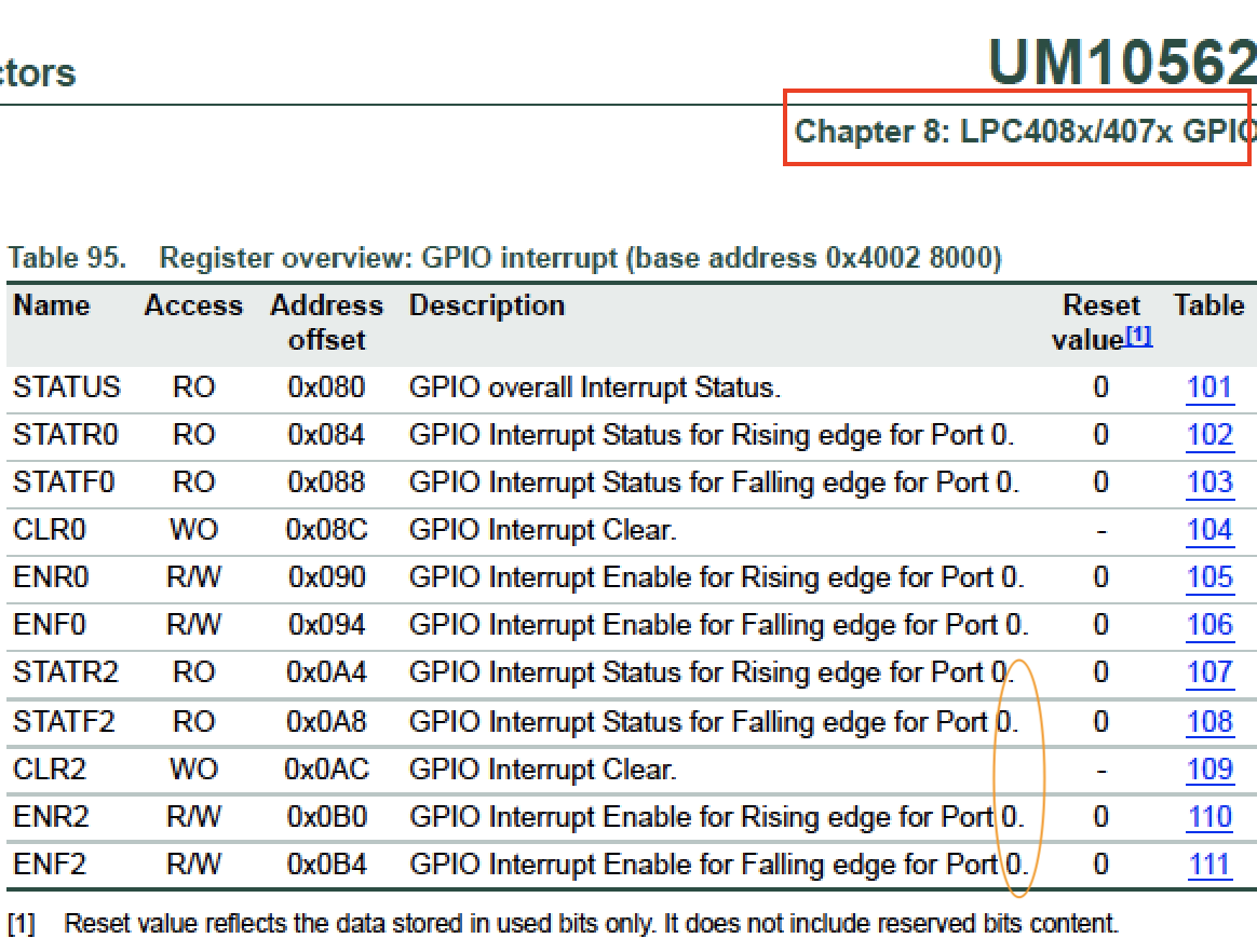
For extra reading material, you can take a look at Chapter 5: LPC408x/407x User Manual, and the Chapter 8 section 8.5.2 to understand more about the GPIO interrupt block diagram

Assignment
Part 0: Simple Interrupt
The first thing you want to do is get a single Port/Pin's interrupt to work without using the RTOS. Make sure you fully understand the following diagram before you proceed. You will configure bits to trigger your GPIO interrupt, and you must also clear bits inside of your GPIO interrupt.
.png)
#include <stdio.h>
#include "lpc40xx.h"
// Step 1:
void main(void) {
// Read Table 95 in the LPC user manual and setup an interrupt on a switch connected to Port0 or Port2
// a) For example, choose SW2 (P0_30) pin on SJ2 board and configure as input
//. Warning: P0.30, and P0.31 require pull-down resistors
// b) Configure the registers to trigger Port0 interrupt (such as falling edge)
// Install GPIO interrupt function at the CPU interrupt (exception) vector
// c) Hijack the interrupt vector at interrupt_vector_table.c and have it call our gpio_interrupt()
// Hint: You can declare 'void gpio_interrupt(void)' at interrupt_vector_table.c such that it can see this function
// Most important step: Enable the GPIO interrupt exception using the ARM Cortex M API (this is from lpc40xx.h)
NVIC_EnableIRQ(GPIO_IRQn);
// Toggle an LED in a loop to ensure/test that the interrupt is entering ane exiting
// For example, if the GPIO interrupt gets stuck, this LED will stop blinking
while (1) {
delay__ms(100);
// TODO: Toggle an LED here
}
}
// Step 2:
void gpio_interrupt(void) {
// a) Clear Port0/2 interrupt using CLR0 or CLR2 registers
// b) Use fprintf(stderr) or blink and LED here to test your ISR
}
Part 1: Interrupt with Binary Semaphore
You will essentially complete Part 0, but with the RTOS using a binary semaphore as a signal to wake a sleeping task. It is recommended to save your code in a separate file (or comment it out), and then start this section of the lab. Do not forget to reference the Semaphore Design Pattern.
For the code that you turn in, you do not have to turn in Part 0 separately since that was just started code for you to get started with the lab. Furthermore, you should improve your code in this part and use the API from lpc_peripherals.h to register your interrupt callback: lpc_peripheral__enable_interrupt(LPC_PERIPHERAL__GPIO, my_gpio_interrupt, "name");
#include "FreeRTOS.h"
#include "semphr.h"
#include "lpc40xx.h"
static SemaphoreHandle_t switch_pressed_signal;
void main(void) {
switch_pressed_signal = ... ; // Create your binary semaphore
configure_your_gpio_interrupt(); // TODO: Setup interrupt by re-using code from Part 0
NVIC_EnableIRQ(GPIO_IRQn); // Enable interrupt gate for the GPIO
xTaskCreate(sleep_on_sem_task, "sem", (512U * 4) / sizeof(void *), NULL, PRIORITY_LOW, NULL);
vTaskStartScheduler();
}
// WARNING: You can only use printf(stderr, "foo") inside of an ISR
void gpio_interrupt(void) {
fprintf(stderr, "ISR Entry");
xSemaphoreGiveFromISR(switch_pressed_signal, NULL);
clear_gpio_interrupt();
}
void sleep_on_sem_task(void * p) {
while(1) {
// Use xSemaphoreTake with forever delay and blink an LED when you get the signal
}
}
Part 2: Support GPIO interrupts using function pointers
In this part, you will use the main GPIO interrupt to be able to dispatch user registered interrupts per pin.
You are designing a library that will allow the programmer to be able to "attach" a function callback to any and each pin on Port 0. Implement all methods and it should work as per the description mentioned in the comments above each function declaration.
// Objective of the assignment is to create a clean API to register sub-interrupts like so:
void pin30_isr(void) { }
void pin29_isr(void) { }
// Example usage:
void main(void) {
gpio0__attach_interrupt(30, GPIO_INTR__RISING_EDGE, pin30_isr);
gpio0__attach_interrupt(29, GPIO_INTR__FALLING_EDGE, pin29_isr);
}Here is starter code for you that demonstrates the use of function pointers:
// @file gpio_isr.h
#pragma once
typedef enum {
GPIO_INTR__FALLING_EDGE,
GPIO_INTR__RISING_EDGE,
} gpio_interrupt_e;
// Function pointer type (demonstrated later in the code sample)
typedef void (*function_pointer_t)(void);
// Allow the user to attach their callbacks
void gpio0__attach_interrupt(uint32_t pin, gpio_interrupt_e interrupt_type, function_pointer_t callback);
// Our main() should configure interrupts to invoke this dispatcher where we will invoke user attached callbacks
// You can hijack 'interrupt_vector_table.c' or use API at lpc_peripherals.h
void gpio0__interrupt_dispatcher(void) {
}And here is the sample code for the implementation:
// @file gpio_isr.c
#include "gpio_isr.h"
// Note: You may want another separate array for falling vs. rising edge callbacks
static function_pointer_t gpio0_callbacks[32];
void gpio0__attach_interrupt(uint32_t pin, gpio_interrupt_e interrupt_type, function_pointer_t callback) {
// 1) Store the callback based on the pin at gpio0_callbacks
// 2) Configure GPIO 0 pin for rising or falling edge
}
// We wrote some of the implementation for you
void gpio0__interrupt_dispatcher(void) {
// Check which pin generated the interrupt
const int pin_that_generated_interrupt = logic_that_you_will_write();
function_pointer_t attached_user_handler = gpio0_callbacks[pin_that_generated_interrupt];
// Invoke the user registered callback, and then clear the interrupt
attached_user_handler();
clear_pin_interrupt(pin_that_generated_interrupt);
}
Below image shows the software workflow. Click on the image below to view animation and understand more on how the driver should work.
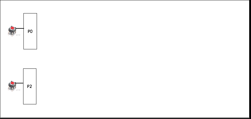
Extra Credit
There are a number of ways to go the extra step and separate yourself from an average student. For this lab, you can do several things to earn extra credit:
- Go back to the previous lab, and instead of implementing a task that reads input, design it such that it registers a callback instead.
- Improve the code quality. Instead of hacky code that barely works, demonstrate your code quality by making your code more robust and clean.
-
You can extend your API in
Part 2to also supportPort 2
Requirements
- You should be able to fully re-write code for
Part 0orPart 1, meaning that you understand the code that you just wrote. You are encouraged to ask questions for any line of code that is not well understood (or magical). - Should be able to specify a callback function for any pin for an exposed GPIO given a rising or falling condition
- We may ask you to change which pin causes a particular callback to be executed in your code and then recompile and re-flash your board to and prove it works with any pin
Note that printing 4 chars inside an ISR can take 1ms at 38400bps, and this is an eternity for the processor and should never be done (other than todebug)
What to turn in:
- Place all relevant source files within a .pdf file.
- Turn in the screenshots of terminal output.
Lesson ADC + PWM
Pin Selection and Pin Mode
Objective
Know how to select a specific functionality of a given LPC40xx pin. Know how to select a pin mode.
Pin Selection
Every GPIO pin of the LPC40xx is capable of other alternative functionalities. Pin selection is the method by which a user is able to designate the functionality of any given pin. For example, GPIO Pin 0.0 can alternatively be used for CAN channel 1 receive, UART channel 3 transmit, and I2C channel 1 data line.
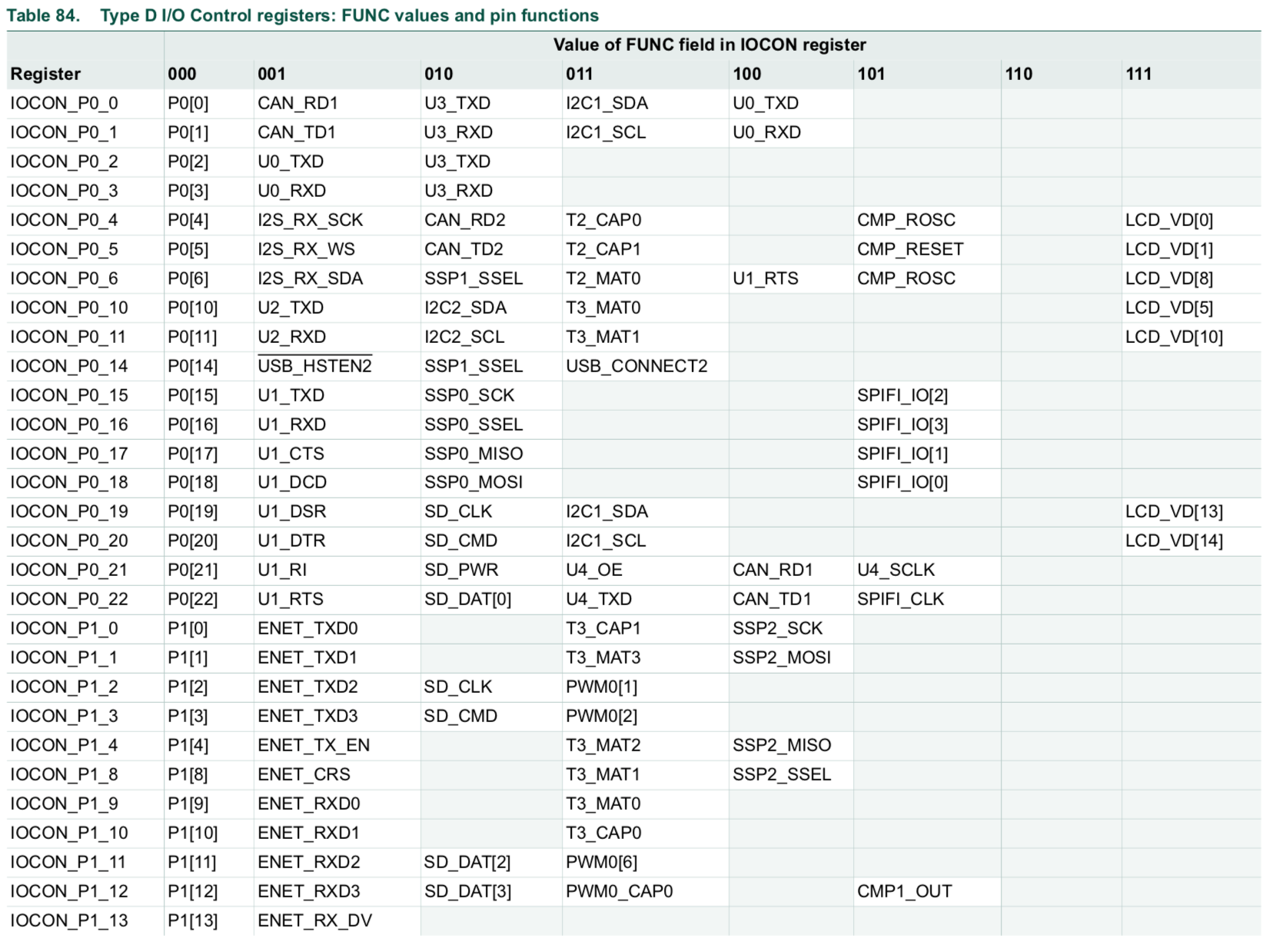
Figure 1A. LPC40xx User Manual IOCON

Figure 1B. I/O Pin Select Mux (from LPC2148, for illustration purposes only)
In order to select the I2C2_SDA functionality of pin 0.10, one must set bit 1, reset bit 0 & 3 of the IOCON register function field to 010.
// Using LPC40xx.h pointers
LPC_IOCON->P0_10 &= ~0b010 // reset all bits of function[2:0]
LPC_IOCON->P0_10 |= 0b010; // set the function bit for I2C2Pin Mode
The LPC17xx has several registers dedicated to setting a pin's mode. Mode refers to enabling/disabling pull up/down resistors as well as open-drain configuration. PINMODE registers allow users to enable a pull-up (00), enable pull up and pull down (01), disable pull up and pull down (10), and enable pull-down (11). PINMODE_OD registers allow users to enable/disable open-drain mode.

Figure 2. LPC17xx User Manual PINMODE & PINMODE_OD

Figure 3. LPC17xx User Manual PINMODE0

Figure 4. LPC17xx User Manual PINMODE_OD0
For example, if one desires to configure pin 0.09 to enable a pull-up resistor and open drain mode, one must clear bits 18 & 19 of PINMODE0 register, and set bit 9 of register PINMODE_OD0.
// Using the memory address from the datasheet
*(0x4002C040) &= ~(0x3 << 18); // Clear bits 18 & 19
*(0x4002C068) |= (0x1 << 9); // Set bit 9
// Using LPC17xx.h pointers
LPC_PINCON->PINMODE0 &= ~(0x3 << 18); // Clear bits 18 & 19
LPC_PINCON->PINMODE_OD0 |= (0x1 << 9); // Set bit 9
You may find it helpful to automate register setting and/or clearing. Per our Coding Standards, inline functions should be used (not Macros).

Figure 5. LPC17xx Pin Registers & Circuit (credit: https://sites.google.com/site/johnkneenmicrocontrollers/input_output/io_1768)
ADC (Analog to Digital Converter)
Objective
To learn about the use of ADCs, their different types, their related parameters, and how to set up an ADC driver for the LPC40xx.
What does ADC accomplish?
An Analog to Digital Converter is needed whenever one needs to interface a digital system with an analog device. For example, if one needs to read the voltage across a resistor, and use the value within an algorithm running on the SJOne board, an ADC circuit is needed to convert the analog voltage to a discrete digital value. Luckily, the LPC40xx, like most microcontrollers, includes an ADC circuit that we can utilize.
Different types of ADC circuits
Flash ADC
The simplest and fastest ADC circuit relies on a series of comparators that compare the input voltage to a range of voltage reference values. The digital output of the comparators is wired to a priority encoder. The output of the priority encoder represents the binary value of the input voltage.
Note that the number of bits of the binary output (n) requires (2n-1) comparators. Therefore, the circuit complexity grows exponentially with respect to the number of bits used to represent the converted value (resolution).

Figure 1. Flash ADC Circuit (credit: allaboutcircuits.com)

Figure 2. Flash ADC Timing (credit: allaboutcircuits.com)
Digital Ramp ADC
This type of ADC utilizes an up counter, a comparator, a DAC, and a register. DACs (Digital Analog Converters), as their name suggests, perform the inverse operation of an ADC, i.e. They convert a binary input into an analog voltage output. The up counter starts at zero and counts up synchronously. The output of the counter is wired to the DAC. The analog output of the DAC is compared to the analog input signal. As long as the comparator indicates that the input voltage is larger than the DAC's value, the counter continues to increment. Eventually, the DAC's output will exceed the input voltage, and the comparator will activate the counter's reset signal as well as the register's load signal. The register's output represents the binary value of the input analog signal.
Note that because the counter starts from zero with every sample, the time it takes the circuit to produce the digital output is inconsistent.

Figure 3. Digital Ramp ADC Circuit (credit: allaboutcircuits.com)

Figure 4a. Digital Ramp ADC Timing (credit: allaboutcircuits.com)

Figure 4b. Digital Ramp ADC Timing Variance (credit: allaboutcircuits.com)
Successive Approximation ADC
A successive approximation ADC works very similarly to a digital ramp ADC, except it utilizes a successive approximation register (SAR) in place of the counter. The SAR sets each bit from MSB to LSB according to its greater/less than logic input signal.
This type of ADC is more popular than flash and digital ramp due to its consistent timing and relatively scalable design.

Figure 5. Successive Approximation ADC Circuit (credit: allaboutcircuits.com)

Figure 6. Successive Approximation ADC Timing (credit: allaboutcircuits.com)
Tracking ADC
A Tracking ADC works similarly to the Digital Ramp ADC, except instead of an up counter, it utilizes an up-down counter. The output of the comparator determines whether the counter increments or decrements. It doesn't use a register to hold the processed value since it's constantly tracing the input value.
Note that this type of ADC does not respond well to large changes of the input analog signal. Additionally, it suffers from constantly going over and under the input value. This is known as bit bobble.

Figure 7. Tracking ADC Circuit (credit: allaboutcircuits.com)

Figure 8. Tracking ADC Timing (credit: allaboutcircuits.com)
DAC-free ADCs
Besides Flash ADC, all previous ADC circuits rely on using DACs to convert an estimated digital value to an analog one and compare it to the input signal. There are other types of ADC technologies that do not use DACs. They rely on the known time it takes an RC circuit to discharge to match the input analog signal. Single Slope, Dual Slope, and Delta-Sigma ADCs implement this concept.
ADC Parameters
Resolution
This is typically the most-highlighted aspect of any ADC technology. Resolution refers to the number of bits of the ADC's output. It's a measurement of how coarse/fine the converted value is. A four bit 5V ADC offers 16 values for the voltage range 0 V to 5 V (i.e. roughly 312 mV per bit increment). A 10 bit 5V ADC offers 1024 values for the same voltage range (roughly 5 mV per bit increment).
Sampling Frequency
This is simply the circuit's latency (i.e. the rate of converting an analog input signal to digital bits). The highest frequency of an analog signal that a given ADC circuit is able to adequately capture is known as Nyquist frequency. Nyquist frequency is equal to one-half of the circuits sampling frequency. Therefore, to adequately convert an analog signal of frequency n Hz, one must have an ADC circuit with 2n Hz sampling frequency. Otherwise, aliasing happens. Aliasing occurs when an ADC circuit samples an input signal too slowly, thus producing an output signal that is not the true input signal, but rather an alias of it.

Figure 9. ADC Aliasing
Step Recovery
This is a measurement of how quickly an ADC's output is able to respond to a sudden change in input. For example, flash and successive approximation ADCs are able to adjust relatively quickly to input changes while tracking ADC struggles with large input changes.
Range
This is a measurement of the range of voltages that an ADC circuit is able to capture and output. For example, the LPC40xx has a range of 0V to 3.3V. Other ADCs may have bigger ranges or even variable ranges that a user can select, such as this device: https://www.mouser.com/ds/2/609/AD7327-EP-916882.pdf
Error
This is a measurement of the systematic error of any given ADC circuit. This is measured by comparing the actual input signal to its digital output equivalent. Note that, this error measurement is only valid within the range of the ADC in question.
ADC Driver for LPC40xx
Figure 10. LPC40xx User Manual ADC Instructions
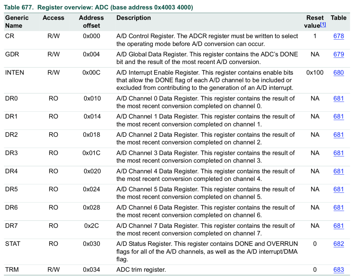
Figure 11. LPC40xx User Manual ADC Control Register
PWM (Pulse Width Modulation)
Objective
To learn about the use of PWM signals, their related parameters, and how to set up an ADC driver for the LPC40xx.
What is a PWM signal?
A Pulse Width Modulation (PWM) signal is simply a digital signal that is on (high) for part of its period and off (low) for the remainder of its period. If such a signal is on half the time and off the other half, then it's a square wave.
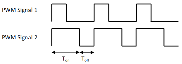
Figure 1. PWM Signal (credit: www.bvsystems.be)
PWM Parameters
Duty Cycle
A duty cycle of a certain PWM signal is given as a percentage, and it represents the ratio of the signal "on" time to the signal's full period. In other words, if the duty cycle of a signal is said to be 75%, it means that this signal is high for 75% of its period and low for the remaining 25%. 100% duty cycle implies a constantly high signal, and a 0% duty cycle implies a constantly grounded signal.
Frequency
The frequency of a PWM signal (just like any electrical signal) refers to the rate at which the signal repeats per second. A 1 Hz signal repeats every 1 second while a 1 kHz signal repeats every 1 millisecond.

Figure 2. Parameters of a PWM signal
PWM Signal Applications
Generally speaking, a PWM signal is a way for a digital system to interface with an analog device.
DC Motors
DC Motors are controllable via a PWM signal. The duty cycle of the signal is typically linearly proportional to the velocity of the motor. For example, a 60 RPM motor driven by a 50% duty cycle PWM signal will rotate at a 30 RPM velocity. It's worth noting that such a signal needs to run at a high enough frequency (10 kHz for example) so the motor can rotate smoothly. A low-frequency PWM signal (say 10 Hz) will result in an observable choppy motor motion.
LEDs
The brightness of an LED can be controlled via a reasonably high-frequency PWM signal. A 5V 50% PWM signal applied to an LED will have the same brightness effect as a constant 2.5V signal applied to the same LED.
Servos
Servos are typically controlled by a 50 Hz PWM signal, where the duty cycle of the signal determines the angle of the servo. Typically, the duty cycle ranges from 5% to 10%, causing the servo to rotate to its smallest and largest angles, respectively.
PWM Driver for LPC40xx

Theory of Operation
Behind every PWM is a Peripheral (HW) counter (TC). For "Single Edge" PWM, when the counter starts from zero, the output of the PWM (GPIO) can reset back to logical 1. Then, when the value of the "Match Register (MR)" occurs, then the PWM output can set to logical 0. Therefore, the maximum limit of the TC controls the frequency of the PWM signal, and the MR registers control the duty cycle.

Software PWM
This section demonstrates the LPC PWM operation in software. The LPC processor implements similar code, but in the hardware.
void lpc_pwm(void)
{
bool GPIO_PWM1 = true; // Hypothetical GPIO that this PWM channel controls
uint32_t TC = 0; // Hardware counter
uint32_t MR0 = 500; // TC resets when it matches this
// Assumptions: SW instructions add no latency, and delay_us() is the only instruction that takes time
while (1)
{
if (++TC >= MR0) {
TC = 0;
GPIO_PWM1 = true; // GPIO is HIGH on the reset of TC
}
if (TC >= MR1) {
GPIO_PWM1 = false; // GPIO resets upon the match register
}
// 1uS * 500 = 500uS, so 2Khz PWM
delay_us(1);
}
}Registers of relevance
What you are essentially trying to control is the PWM frequency and the PWM duty cycle. For instance, a 50% duty cycle with just a 1Hz PWM will blink your LED once a second. But a 50% duty cycle 1Khz signal will dim your LED to 50% of the total brightness it is capable of. There are "rules" that the PWM module uses to alter a GPIO pin's output and these rules are what you are trying to understand. So read up on "Rules of Single Edge Conrolled PWM" in your datasheet and overall the LPC PWM chapter at minimum 10 times to understand it. You may skip the sections regarding "capture", and "interrupts". Furthermore, to use the simplified PWM, you can use the Single Edge PWM rather than the more complex Double Edge because the Single Edge edge PWM is controlled by a dedicated MR register.
TC, MR0, MCR and PR: The Prescalar (PR) register controls the tick rate of the hardware counter that can alter the frequency of your PWM. For instance, when the CPU clock is 10Mhz, and the PR = 9, then the TC counts up at the rate of 10/(9+1) = 1 Mhz. Hence, the PR affects the frequency, but we still need a "max count" to set the frequency with precision. So if the TC increments at 1Mhz, and MR0 is set to 100, then you will have 1000Khz/100 = 10Khz PWM.
The MCR register controls what happens to the TC when a match occurs. The one subtle, but important thing we need to do is that when the MR0 match occurs, we need the TC to reset to zero to be able to use MR0 as a frequency control.
TCR and PCR: The PCR register enables the channels, so if you have PWM1.4 as an output, that means you need to enable channel 4. The TCR register is a key register that will enable your PWM module.
Lab: ADC + PWM
Objective
Improve an ADC driver, and use an existing PWM driver to design and implement an embedded application, which uses RTOS queues to communicate between tasks.
This lab will utilize:
- ADC Driver
- You will improve the driver functionality
- You will use a potentiometer that controls the analog voltage feeding into an analog pin of your microcontroller
- PWM Driver
- You will use an existing PWM Driver to control a GPIO
- An led brightness will be controlled, or you can create multiple colors using an RGB LED
- FreeRTOS Tasks
- You will use FreeRTOS queues
Assignment
Preparation:
Before you start the assignment, please read the following in your LPC User manual (UM10562.PDF)
- Chapter 7: I/O configuration
- Chapter 32: ADC
Part 0: Use PWM1 driver to control a PWM output pin
The first thing to do is to select a pin to function as a PWM signal. This means that once you select a pin function correctly, then the pin's function is controlled by the PWM peripheral and you cannot control the pin's HIGH or LOW using the GPIO peripheral. By default, a pin's function is as GPIO, but for example, you can disconnect this function and select the PWM function by using the IOCON_P2_0

- Re-use the PWM driver
- Study the
pwm1.handpwm1.cfiles underl3_driversdirectory
- Study the
- Locate the pins that the PWM peripheral can control at
Table 84: FUNC values and pin functions- These are labeled as
PWM1[x]wherePWM1is the peripheral, and[x]is a channel- So
PWM1[2]means PWM1, channel 2
- So
- Now find which of these channels are available as a free pin on your SJ2 board and connect the RGB led
- Set the
FUNCof the pin to use this GPIO as a PWM output
- Set the
- These are labeled as
- Initialize and use the PWM-1 driver
- Initialize the PWM1 driver at a frequency of your choice (greater than 30Hz for human eyes)
- Set the duty cycle and let the hardware do its job :)
- You are finished with Part 0 if you can demonstrate control over an LED's brightness using the HW based PWM method
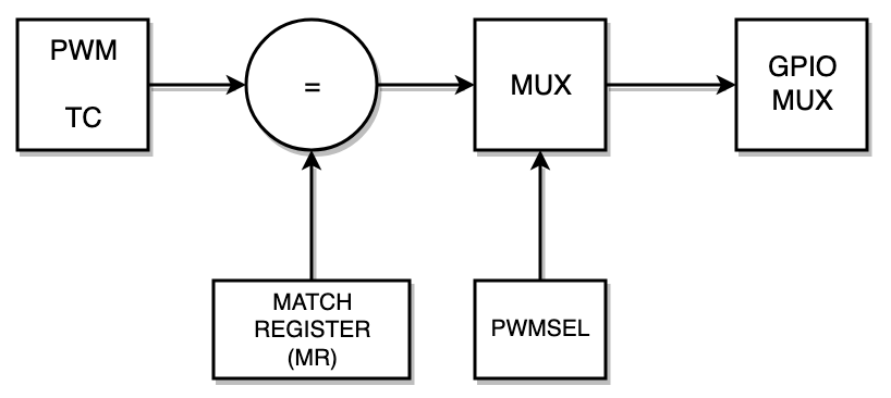
#include "pwm1.h"
#include "FreeRTOS.h"
#include "task.h"
void pwm_task(void *p) {
pwm1__init_single_edge(1000);
// Locate a GPIO pin that a PWM channel will control
// NOTE You can use gpio__construct_with_function() API from gpio.h
// TODO Write this function yourself
pin_configure_pwm_channel_as_io_pin();
// We only need to set PWM configuration once, and the HW will drive
// the GPIO at 1000Hz, and control set its duty cycle to 50%
pwm1__set_duty_cycle(PWM1__2_0, 50);
// Continue to vary the duty cycle in the loop
uint8_t percent = 0;
while (1) {
pwm1__set_duty_cycle(PWM1__2_0, percent);
if (++percent > 100) {
percent = 0;
}
vTaskDelay(100);
}
}
void main(void) {
xTaskCreate(pwm_task, ...);
vTaskStartScheduler();
}
Part 1: Alter the ADC driver to enable Burst Mode
- Study
adc.handadc.cfiles inl3_driversdirectory and correlate the code with the ADC peripheral by reading the LPC User Manual.- Do not skim over the driver, make sure you fully understand it.
- Identify a pin on the SJ2 board that is an ADC channel going into your ADC peripheral.
- Reference the I/O pin map section in
Table 84,85,86: FUNC values and pin functions
- Reference the I/O pin map section in
- Connect a potentiometer to one of the ADC pins available on SJ2 board. Use the ADC driver and implement a simple task to decode the potentiometer values and print them. Values printed should range from 0-4095 for different positions of the potentiometer.
// TODO: Open up existing adc.h file
// TODO: Add the following API
/**
* Implement a new function called adc__enable_burst_mode() which will
* set the relevant bits in Control Register (CR) to enable burst mode.
*/
void adc__enable_burst_mode(void);
/**
* Note:
* The existing ADC driver is designed to work for non-burst mode
*
* You will need to write a routine that reads data while the ADC is in burst mode
* Note that in burst mode, you will NOT read the result from the GDR register
* Read the LPC user manual for more details
*/
uint16_t adc__get_channel_reading_with_burst_mode(uint8_t channel_number);
#include "adc.h"
#include "FreeRTOS.h"
#include "task.h"
void adc_pin_initialize(void) {
// TODO: Ensure that you also set ADMODE to 0
// TODO: Ensure you set pull/up and pull/down bits 0
// TODO: Then use gpio__construct_with_function(...)
}
void adc_task(void *p) {
adc_pin_initialize();
adc__initialize();
// TODO This is the function you need to add to adc.h
// You can configure burst mode for just the channel you are using
adc__enable_burst_mode();
// Configure a pin, such as P1.31 with FUNC 011 to route this pin as ADC channel 5
// You can use gpio__construct_with_function() API from gpio.h
pin_configure_adc_channel_as_io_pin(); // TODO You need to write this function
while (1) {
// Get the ADC reading using a new routine you created to read an ADC burst reading
// TODO: You need to write the implementation of this function
const uint16_t adc_value = adc__get_channel_reading_with_burst_mode(ADC__CHANNEL_2);
vTaskDelay(100);
}
}
void main(void) {
xTaskCreate(adc_task, ...);
vTaskStartScheduler();
}
Part 2: Use FreeRTOS Queues to communicate between tasks
- Read this chapter to understand how FreeRTOS queues work
- Send data from the
adc_taskto the RTOS queue - Receive data from the queue in the
pwm_task
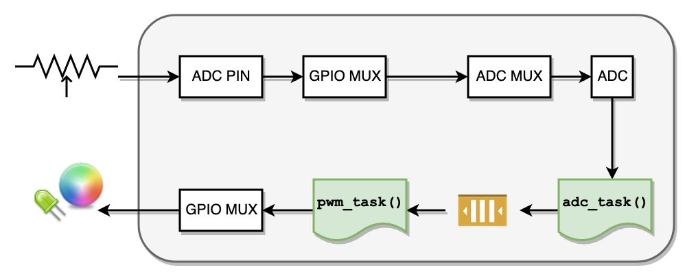
#include "adc.h"
#include "FreeRTOS.h"
#include "task.h"
#include "queue.h"
// This is the queue handle we will need for the xQueue Send/Receive API
static QueueHandle_t adc_to_pwm_task_queue;
void adc_task(void *p) {
// NOTE: Reuse the code from Part 1
int adc_reading = 0; // Note that this 'adc_reading' is not the same variable as the one from adc_task
while (1) {
// Implement code to send potentiometer value on the queue
// a) read ADC input to 'int adc_reading'
// b) Send to queue: xQueueSend(adc_to_pwm_task_queue, &adc_reading, 0);
vTaskDelay(100);
}
}
void pwm_task(void *p) {
// NOTE: Reuse the code from Part 0
int adc_reading = 0;
while (1) {
// Implement code to receive potentiometer value from queue
if (xQueueReceive(adc_to_pwm_task_queue, &adc_reading, 100)) {
}
// We do not need task delay because our queue API will put task to sleep when there is no data in the queue
// vTaskDelay(100);
}
}
void main(void) {
// Queue will only hold 1 integer
adc_to_pwm_task_queue = xQueueCreate(1, sizeof(int));
xTaskCreate(adc_task, ...);
xTaskCreate(pwm_task, ...);
vTaskStartScheduler();
}
Part 3: Allow the Potentiometer to control the RGB LED
At this point, you should have the following structure in place:
- ADC task is reading the potentiometer ADC channel, and sending its values over to a queue
- PWM task is reading from the queue
Your next step is:
- PWM task should read the ADC queue value, and control the an LED
Final Requirements
Minimal requirement is to use a single potentiometer, and vary the light output of an LED using a PWM. For extra credit, you may use 3 PWM pins to control an RGB led and create color combinations using a single potentiometer.
- Make sure your Part 3 requirements are completed
-
pwm_taskshould print the values of MR0, and the match register used to alter the PWM LEDs- For example, MR1 may be used to control P2.0, so you will print MR0, and MR1
- Use memory mapped
LPC_PWMregisters fromlpc40xx.h
- Make sure BURST MODE is enabled correctly.
-
adc_taskshould convert the digital value to a voltage value (such as 1.653 volts) and print it out to the serial console- Remember that your VREF for ADC is 3.3, and you can use ratio to find the voltage value
adc_voltage / 3.3 = adc_reading / 4095
Lesson SPI
SPI (Serial & Peripheral Interface)
What is SPI
SPI is a high-speed, full-duplex bus that uses a minimum of 3 wires to exchange data (and a number of device-selected wires). The popularity of this bus rose when SD cards (and its variants ie: micro-sd) officially supported this bus according to the SD specifications. SPI allows microcontrollers to communicate with multiple slave devices.
SPI Bus Signals

Figure 1. SPI Signals
| MASTER Pin Name | SLAVE Pin Name | Pin Function |
| MOSI | SI | Master Out Slave In (driven by master), this pin is used to send sends data to the slave device. |
| MISO | SO | Master In Slave Out (driven by slave), this pin is used by the slave to send data to the master device. |
| SCLK | CLK | Serial Clock (driven by master), clock that signals when to read MISO and MOSI lines |
| CS | CS | Chip Select (driven by master), used to indicate to the slave that you want to talk to it and not another slave device. This will activate the slave's MISO line. MISO line is set to h-z if this is not asserted. MISO is set to high if this signal is asserted. |
| INT | Interrupt (Optional) (driven by slave), an interrupt signal to alert the master that the slave device wants to communicate. Not all devices have this. This is not always needed. This is not apart of the standard. |
The SCK signal can reach speed of 24Mhz and beyond, however, SD cards are usually limited to 24Mhz according to the specifications. Furthermore, any signal over 24Mhz on a PCB requires special design consideration to make sure it will not deteriorate, thus 24Mhz is the usual maximum. Furthermore, you need a CPU twice as fast as the speed you wish to run to support it. For example, to run at 24Mhz SPI, we need 48Mhz CPU or higher. Because each wire is driven directly (rather than open-collector), higher speeds can be attained compared to 400Khz I2C bus.
Multi-slave bus
Suppose that you wanted to interface a single SPI bus to three SD cards, the following will need to be done :
- Connect all MOSI, MISO, and SCK lines together
- Connect individual CS lines of three SD cards to SPI master (your processor)
It is also recommended to provide a weak pull-up resistor on each of the SPI wires otherwise some devices like an SD card may not work. 50K resistor should work, however, lower resistor value can achieve higher SPI speeds.

Figure 2. Typical SPI Bus (wikipedia SPI, user Cburnett)
As a warning, if your firmware selects more than one SPI slave chip select, and they both attempt to drive the MISO line, since those lines are totem-pole (push-pull), there will be bus contention and could possibly destroy both SPI devices.
The "CS" section of the SPI/SSP chapter describes the information if your microcontroller is going to be a slave on the SPI bus. Since your LPC micro is a master in reality, please do not confuse the CS pin for the SPI slave functionality. Even if the CS pin is actually used to CS the Adesto flash, it is just an ordinary GPIO and will not function as the one described in your SPI/SSP chapter.
Therefore, do not configure the "SSEL" in your PINSEL (or PIN function) since that is reserved for the case when your micro is an SPI Slave. In your case, the same GPIO that has the "SSEL" capability is a simple GPIO to control the CS of the SPI Flash memory.
SPI Timing Diagram

Figure 3. SPI timing diagram
SPI has a few timing modes in which data is qualified on the rising or falling edge. In this case, and most, we qualify the MOSI and MISO signals on the rising edge. For a whole transaction to be qualified, the ~CS must be asserted. When the CS pin is pulled high (deasserted), the transaction is over and another transaction can be performed. This must be done for each transaction done by the master to the slave.
The SPI is labeled as SSP on LPC17xx or LPC40xx User Manual due to historic reasons, and this chapter in the datasheet shows the software setup very well. After the SPI is initialized on the hardware pins, the next steps is to write an SPI function that will exchange a byte. Note that if the master wants to receive data, it must send a data byte out to get a data byte back. The moment we write to the DR (data register) of the SPI peripheral, the MOSI will begin to send out the data. At the same time, the MISO will capture the data byte back to the same DR register. In other words, SPI bus is a forced full-duplex bus.
Ensure that two transactions with the SPI device do not occur back to back without a delay. For instance, insert at least 1uS delay between successive DS and CS of another transaction.
Why use SPI
Pros
-
High Speed:
- There is no standard speed limit for SPI beyond how fast a Single-Ended Signal can propagate and how fast an SPI compatible device can react.
- In other words, how fast can you talk over a wire and how fast can a slave device read a clock signal.
-
Simple:
- Doesn't require special timing or a special state-machine to run. It doesn't really need hardware peripheral either. It can be bit-banged via GPIO.
-
Synchronous:
- This communication standard utilizes a clock to qualify signals.
-
Full-Duplex:
- Communication both ways. The slave to speak to the master at the same time that the master can speak to the slave device.
-
Multi-slave:
- You can talk to as many slaves as you have chip selects.
Cons
-
IO/Pin Count:
- IO count increases by one for each slave device you introduce, since each slave device needs a chip select.
- You also almost always need at least 4 wires for this communication protocol.
- There are some special cases that do not fit this but they are uncommon.
-
Master Only Control:
- Although the communication protocol can allow for full-duplex communication, the only way for a slave device to be able to communicate with the master is if the master initiates communication.
- A slave can only speak when spoken to.
Software Driver
Preparation for the SPI driver
- Note that when we refer to SPI, we are referring to the SSP peripheral in the LPC user manual.
- SSP stands for Synchronous Serial Protocol and SPI is one of the synchronous serial protocols it can perform.
- Study the schematic, and take a note of which pins have the SSP2 or SPI#2 peripheral pin-out.
- Note this down or draw this out.
- Study and read the SSP2 LPC user manual chapter a few times
- Study the schematic, and locate the CS pin for the SPI flash attached to SSP2, then write a simple GPIO driver for this to select and deselect this pin
- Read the SPI flash datasheet that shows the SPI transactions for read/write, signature read etc.
- Rev.4 board has Adesto flash, and previous revisions have Atmel flash.
Multitasking Warnings: if your software runs multiple tasks, and these tasks can access SPI, care needs to be taken because if two CS signals are asserted at the same time, hardware damage will occur. This leads to the topic of using a mutex (semaphore) under FreeRTOS and you can read the FreeRTOS tutorial to learn more.
Set the clock rate to be below the specification of the SPI device you are interfacing.
Mutexes
Binary Semaphore vs Mutex
Binary semaphores and a mutex are nearly the same constructs except that a mutex have the feature of priority inheritance, where in a low priority task can inherit the priority of a task with greater priority if the higher priority task attempts to take a mutex that the low priority task possess.
This article provides a quick review on Binary Semaphore, Mutex, and Queue.
Priority Inversion Using a Semaphore
Below is an illustration of the scenario where using a semaphore can cause priority inversion.
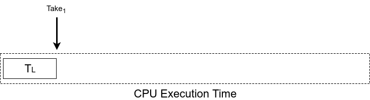
Figure 1. Low priority task is currently running and takes a semaphore.
.png)
Figure 2. OS Tick event occurs.
.png)
Figure 3. High priority task is ready to run and selected to run.
.png)
Figure 4. High priority task attempts to take semaphore and blocks.
.png)
Figure 5. Since high priority task is blocked, the next ready task that can run is the low priority task. The OS tick event occurs.
.png)
Figure 6. The OS tick event occurs, a middle priority task, that never sleeps is ready to run, it begins to run, high priority task is blocked on semaphore and low priority task is blocked by the middle priority task. This is priority inversion, where a medium priority task is running over a higher priority task.
Priority Inheritance using Mutex
Priority inheritance is the means of preventing priority inversion.
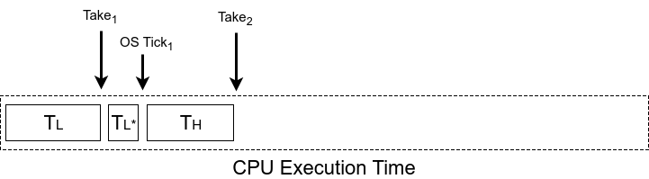
Figure 7. Moving a bit further, the high priority task attempts to take the Mutex
.png)
Figure 8. Low priority task inherates the highest priority of the task that attempts to take the mutex it posses.
.png)
Figure 9. OS Tick2 occurs, and medium priority task is ready, but the low priority task has inheritated a higher priority, thus it runs above the medium priority task.
.png)
Figure 10. Low priority task gives the mutex, low priority task de-inheritates its priority, and the high task immediately begins to run. It will run over the medium task.
.png)
Figure 11. At give2 high priority task releases the mutex and sleeps. Some time elapses, and then the medium task begins to run. No priority inversion occurs in this scenario, the RTOS rule of highest priority runs first is held.
Design Pattern
The design pattern for a mutex should be exclusively used as a protection token. Mutexes can be used in place of as semaphores but the addition work of priority inheritance will cause this approach to take longer and thus be less efficient than a semaphore.
#include "FreeRTOS.h"
#include "semphr.h"
// In main(), initialize your Mutex:
SemaphoreHandle_t spi_bus_mutex = xSemaphoreCreateMutex();
void task_one()
{
while(1) {
if(xSemaphoreTake(spi_bus_mutex, 1000)) {
// Use Guarded Resource
// Give Semaphore back:
xSemaphoreGive(spi_bus_mutex);
}
}
}
void task_two()
{
while(1) {
if(xSemaphoreTake(spi_bus_mutex, 1000)) {
// Use Guarded Resource
// Give Semaphore back:
xSemaphoreGive(spi_bus_mutex);
}
}
}
Other notes
Good APIs actually have protection such that the mutex cannot be given accidentally.
Structured Bit-fields Register Mapping
Please Review the Following
- Structures in C: http://www.cplusplus.com/doc/tutorial/structures/
- Unions in C: http://www.cplusplus.com/doc/tutorial/other_data_types/
Register Structure Mapping
Lets observe the status register for the ADXL362 accelerometer. The choice of this device is arbitrary.

Figure 1. ADXL362 Status Register
Normally, and more portably, to store information about the awake bit, you would do the following:
/* Get byte from accelerometer */
uint8_t status = getStatusByte();
/* Store 6th bit using a shift and mask */
bool awake = ((status >> 6) & 0b1);
// You can also do this (to guarantee the result to be true or false only, rather than 0 or (1 << 6) which is 64
bool awake = (status & (1 << 6)) ? true : false;
bool awake = !!(status & (1 << 6));
/* Now use the stored awake boolean */
if(awake)
{
doAThing();
}The above is fine, but it would be great to do this in a more elegant fashion. For example, the following:
/* Get a byte and cast it to our adlx_t structure */
adlx_t status = (adlx_t)getStatusByte();
/* Now retrieve the awake bit using the following syntax */
if(status.awake)
{
doAThing();
}To do something like this, you can define the adlx_t structure in the following way:
typedef struct __attribute__((packed))
{
uint8_t data_ready: 1;
uint8_t fifo_ready: 1;
uint8_t fifo_warning: 1;
uint8_t fifo_overrun: 1;
uint8_t activity: 1;
uint8_t : 1; /* Un-named padding, since I don't care about the inactivity signal */
uint8_t awake: 1;
uint8_t error: 1;
} adlx_t;The colon specifies the start of a bit field. The number after the colon is the length in bits that label will take up. The __attribute__((packed)) is a necessary compiler directive, specific to GCC which tells the compiler to make sure that the structure is packed together in the way that it is shown. It also tells the compiler to not rearrange it or expand it in order to make it more efficient to work with by the CPU.
NOTE: that the bit-field example and the shift and mask example are equivalent computationally. One is not necessarily more efficient the other. On one hand, you are writing the mask, in the other, the compiler does this for you.
Using Unions
Lets say we wanted to set the whole structure to zeros or a specific value, we can do this using unions.
typedef union
{
uint8_t byte;
struct
{
uint8_t data_ready: 1;
uint8_t fifo_ready: 1;
uint8_t fifo_warning: 1;
uint8_t fifo_overrun: 1;
uint8_t activity: 1;
uint8_t inactivity: 1;
uint8_t awake: 1;
uint8_t error: 1;
} __attribute__((packed));
} adlx_t;This allows the user to do the following:
/* Declare status variable */
adlx_t status;
/* Set whole bit field through the byte member */
status.byte = getStatusByte();
/* Use awake bit */
if (status.awake)
{
doSomething();
}
/* Clear bit field */
status.byte = 0;What about large data structures? For example, the ID3v1 metadata structure for MP3 files. This datastructure contains title name, artist and many other bits of information about the song to be played. It contains 128 bytes
| Field | Length | Description |
|---|---|---|
| header | 3 | "TAG" |
| title | 30 | 30 characters of the title |
| artist | 30 | 30 characters of the artist name |
| album | 30 | 30 characters of the album name |
| year | 4 | A four-digit year |
| comment | 28 | The comment. |
| zero-byte | 1 | If a track number is stored, this byte contains a binary 0. |
| track | 1 | The number of the track on the album, or 0. Invalid, if previous byte is not a binary 0. |
| genre | 1 | Index in a list of genres, or 255 |
This is not a bit field, but the same principles stand. This can be turned into a structure as well:
typedef union
{
uint8_t buffer[128];
struct
{
uint8_t header[3];
uint8_t title[30];
uint8_t artist[30];
uint8_t album[30];
uint8_t year[4];
uint8_t comment[28];
uint8_t zero;
uint8_t track;
uint8_t genre;
} __attribute__((packed));
} ID3v1_t;Now, it would take up 128 bytes of memory in to create one of these structures and we want to be conservative. To use use the structure properties, and reduce space usage you can utilize pointers and casting.
ID3v1_t mp3;
/* Some function to get the ID3v1 data */
dumpMP3DataIntoBuffer(&mp3.buffer[0]);
/* Compare string TAG with header member */
printf(" Title: %.30s\n", mp3.title);
printf("Artist: %.30s\n", mp3.artist);Using Macros
Using some casting techniques and macros you can do something like the following:
#define ADLX(reg) (*((adlx_t*)(®)))
uint8_t status = getStatusByte();
if (ADLX(status).awake)
{
doAThing();
}Dangers of Using Bit-fields
The above example that does not use bit-fields is quite portable, but bit-field mapping can be problematic depending on these factors
-
Endianess of your system: If a bit-field of a status register is little-endian and your processor is big-endian, the bits will be flipped.
- This link explains this further: http://opensourceforu.com/2015/03/be-cautious-while-using-bit-fields-for-programming/
- Structure of your struct: in gcc, using __attribute__((packed)) is very important, because the compiler may attempt to optimize that structure for speed, by expanding the members of the struct into 32-bits, or it may reorder the members and bit to make easier to do operations on. In these cases, the mapping will no longer work. This is something to consider when using this. This also typically depends on the compiler options for compiling.
- Mixing bit fields and members: See the link below on some issues that occurred when you mix bit-fields with variables.
Lab: SPI Flash Interface
The objective is to learn how to create a thread-safe driver for Synchronous Serial Port and to communicate with an external SPI Flash device.
This lab will utilize:
- SPI driver (LPC user manual calls SPI as SSP)
- Code interface for the SPI flash
- Basic knowledge of data structures
- Mutex strategy to access the SPI flash safely across multiple tasks (or threads)
- Logic Analyzer capture
Important Reminders
- Do not forget to select the PIN functions such that the peripheral can control SCK, MOSI, and MISO pins
- These should be IOCON registers of LPC40xx
- You will not use the SSEL pin of the SPI driver
- The pin that shows SSEL is actually purposed as a GPIO to select the external SPI flash memory
- SSEL pin is meant for the purpose of your microcontroller acting as a SLAVE but since you are trying to be the master, this SSEL pin does not apply to you. It is instead re-purposed as a GPIO for your SPI flash memory.
- Please read this great article also
Assignment
Part 0: SPI Driver

Preparation:
- Before you start the assignment, please read Chapter 21: SSP in your LPC User manual (
UM10562.pdf). You can skip the sections related to interrupts or the DMA.- From LPC User manual to understand the different registers involved in writing a SSP2 driver
- Refer table 84 from LPC User manual for pin configuration
- From the schematics pdf(
Schematics-RevE.2.pdf), identify the pin numbers connected to flash memory and make a note of it because you will be needing them for pin function configuration - Read the external SPI flash datasheet (
DS-AT25DN256_039.pdf) or (DS-AT25SF041_044) depends on the board.
Implement ssp2_lab.h and ssp2_lab.c
Note that there is already an ssp2.h in your sample project, but you will re-write this driver. Refrain from peeking the existing driver because you will have to re-write more complex drivers during your exams without any reference code. If you get a compiler error about 'duplicate symbol' then please re-name your SSP functions accordingly because this compiler error may be stating that there is existing function with the same name in the SPI driver in another file.
#include <stdint.h>
void ssp2__init(uint32_t max_clock_mhz) {
// Refer to LPC User manual and setup the register bits correctly
// a) Power on Peripheral
// b) Setup control registers CR0 and CR1
// c) Setup prescalar register to be <= max_clock_mhz
}
uint8_t ssp2__exchange_byte(uint8_t data_out) {
// Configure the Data register(DR) to send and receive data by checking the SPI peripheral status register
}
Part 1: SPI Flash Interface
Get the code below to work and validate that you are able to read SPI flash memory's manufacture id and compare it with the SPI flash datasheet to ensure that this is correct.
#include "FreeRTOS.h"
#include "task.h"
#include "ssp2_lab.h"
// TODO: Implement Adesto flash memory CS signal as a GPIO driver
void adesto_cs(void);
void adesto_ds(void);
// TODO: Study the Adesto flash 'Manufacturer and Device ID' section
typedef struct {
uint8_t manufacturer_id;
uint8_t device_id_1;
uint8_t device_id_2;
uint8_t extended_device_id;
} adesto_flash_id_s;
// TODO: Implement the code to read Adesto flash memory signature
// TODO: Create struct of type 'adesto_flash_id_s' and return it
adesto_flash_id_s adesto_read_signature(void) {
//adesto_flash_id_s data = { 0 };
adesto_cs();
{
// Send opcode and read bytes
// TODO: Populate members of the 'adesto_flash_id_s' struct
}
adesto_ds();
//return data;
}
void spi_task(void *p) {
const uint32_t spi_clock_mhz = 24;
ssp2__init(spi_clock_mhz);
// From the LPC schematics pdf, find the pin numbers connected to flash memory
// Read table 84 from LPC User Manual and configure PIN functions for SPI2 pins
// You can use gpio__construct_with_function() API from gpio.h
//
// Note: Configure only SCK2, MOSI2, MISO2.
// CS will be a GPIO output pin(configure and setup direction)
todo_configure_your_ssp2_pin_functions();
while (1) {
adesto_flash_id_s id = adesto_read_signature();
// TODO: printf the members of the 'adesto_flash_id_s' struct
vTaskDelay(500);
}
}
void main(void) {
xTaskCreate(spi_task, ...);
vTaskStartScheduler();
}
Part 2: SPI Flash Interface with a Mutex
- Read the article in this link to understand how a mutex is created and used in a task
- Purposely comment out the task creation of the task from Part 1:
xTaskCreate(spi_task,...) - Study the code below which will attempt to read Adesto flash manufacturer ID in two tasks simultaneously
- Run the following code, and confirm that it fails
- Be sure to initialize your SPI, and CS GPIO as needed
#include "FreeRTOS.h"
#include "task.h"
#include "ssp2_lab.h"
void spi_id_verification_task(void *p) {
while (1) {
const adesto_flash_id_s id = ssp2__adesto_read_signature();
// When we read a manufacturer ID we do not expect, we will kill this task
if (0x1F != id.manufacturer_id) {
fprintf(stderr, "Manufacturer ID read failure\n");
vTaskSuspend(NULL); // Kill this task
}
}
}
void main(void) {
// TODO: Initialize your SPI, its pins, Adesto flash CS GPIO etc...
// Create two tasks that will continously read signature
xTaskCreate(spi_id_verification_task, ...);
xTaskCreate(spi_id_verification_task, ...);
vTaskStartScheduler();
}After you confirm that there is a failure while two tasks try to use the SPI bus, resolve this by using a Mutex:
- Protect your
ssp2__adesto_read_signature()a function such that two tasks will not be able to run this function at the same time. - If implemented correctly, you will not see the error
printf
Part 3: Extra Credit
Develop functionality to be able to read and write a "page" of the SPI flash memory. Here is a sample code that you can reference to send a uint32_t address to the SPI flash with MSB first.
#include <stdint.h>
/**
* Adesto flash asks to send 24-bit address
* We can use our usual uint32_t to store the address
* and then transmit this address over the SPI driver
* one byte at a time
*/
void adesto_flash_send_address(uint32_t address) {
(void) ssp2__exchange_byte((address >> 16) & 0xFF);
(void) ssp2__exchange_byte((address >> 8) & 0xFF);
(void) ssp2__exchange_byte((address >> 0) & 0xFF);
}
Conclusion
Logic Analyzer Hints
Saleae logic analyzer is a high quality USB analyzer, although you can find many copy cats as well. After you install the software, do the following:
- Hook up SCK, MOSI, and MISO to particular colors, and configure these colors by selecting the SPI bus in logic analyzer software (on windows for example)
- Setup a trigger
- You have to setup a "trigger" which will trigger the logic analyzer data capture
- The CS signal transitioning from HIGH to LOW is the right choice, however, the CS signal may not be broken out on a pin header
- To provide a trigger, what you can do is that you can SET and RESET two GPIO pins simultaneously. One pin would be the real pin going to Adesto flash, and the second one is an arbitrary pin which is available on your SJ2 pin header that you can connect to the logic analyzer as a trigger
Saleae logic analyzers are fast, but some others are not as fast. What this means is that you should ensure that your speed of the analyzer is FASTER than the SPI speed that you set. If for example your logic analyzer is only 6Mhz, then you should set your SPI speed slower than 6Mhz otherwise it will not capture the data correctly.
Requirements and what to turn in
- Include all the code you developed in this lab
- Turn in the screenshots of terminal output
- Include Manufacturer ID
- Logic Analyzer Screenshots
- This lab requires logic analyzer screenshots. Visit SCE, CmpE294, to borrow Saleae logic analyzer
- Connect your pins to the SSP2 MISO, MOSI, SCK and CS signals to the logic analyzer, and select the option in Saleae program to decode SPI frames
- In your turned in Canvas artifacts, include the waveform of SPI retrieving manufacture ID
Lab: SPI bus contention with SD Card
Overview
- Build your own SPI2 driver
- You will initialize your pins
- You will initialize SPI2 peripheral
- Using existing driver, validate the micro-SD card API to get "sector count"
- The sector count gives you information about the total capacity of the SD card
- Replace the SD card to use your own functions
- Validate if you are able to read the data correctly
- Produce a deliberate race condition while two tasks are reading the sector count
- Use a mutex to solve the race condition
Part 0: Micro-SD Card
In this part, you will familiarize yourself with the low level functions that use the SPI bus to communicate with the (micro) SD card. You will use pre-existing SPI driver in this part just to prove that you are able to communicate with the SD card.
Inspect the following:
- Do a code walkthrough of the
sd_card.h - Study the
sd_card__ioctl()function - Ensure that your micro-SD card is formatted with FAT32
Insert the SD card, and obtain and print the following information in an RTOS task:
- Sector count
- Sector size
- Block size
- Card Identification Number (
MMC_GET_CID)
Part 1: SPI Driver
In this part, write your own SPI driver. Note that, there is already the ssp2.h driver, but the purpose of this exercise is to get practice writing a driver on your own because you will be tested (and quizzed) on this.
void spi2_power_on(void) {
// TODO: Enable PCONP bit: LPC_SC->PCONP
}
void spi_init(void) {
// TODO:
}
char spi_exchange_byte(char byte_out) {
// TODO: Ask SPI peripheral to start to send the data
// TODO: Wait for transfer to complete
// TODO: Capture the data
}
Part 2: Validate your SPI Driver using Part 0
In this part, you will swap out the existing SPI driver with your hand written driver.
// Open : sd_card_defiines.h
// Swap out existing driver implementation with your own:
#define SD_CARD__TRANSMIT_BYTE(byte) YOUR_ssp2__exchange_byte(byte)
#define SD_CARD__RECEIVE_BYTE() YOUR_ssp2__exchange_byte(0xff)Ensure that you can still read the data from the SD card using your own SPI functions. Note that going through the exercise to develop your own driver is critical, and you don't want to merely copy the existing implementation. Hence, please make sure that you are able to write a driver by reading the datasheet alone.
Part 3: Create race condition
In this part, we will re-use the code from Part-0, but attempt to do so in multiple tasks simultaneously.
static void sd_card_read_task(void *p) {
while (1) {
// TODO: Read SD card parameters
// Print them out
// TODO: Add a small amount of sleep
}
}
void main(void) {
// Create two reader tasks that will attempt to read the SPI bus at the same time
xTaskCreate(sd_card_read_task, "sd", 4000/sizeof(void*), NULL, PRIORITY_LOW, NULL);
xTaskCreate(sd_card_read_task, "sd", 4000/sizeof(void*), NULL, PRIORITY_LOW, NULL);
vTaskStartScheduler();
}Part 4: Mutex to the rescue
In this part, solve the race condition issue by using the SD card. Simply surround the critical section of the code that you don't want to access in multiple tasks. See the following pages for reference:
For bonus points, can you figure out how the File I/O is race condition free that uses the SD card APIs? For example, try reading or writing files simultaneously in multiple tasks and you will notice that the code works robustly. Can you figure out the mutex that the File I/O APIs use to solve this problem?
Lesson UART
Clock Systems and Timing
Clock System & Timing
A crystal oscillator is typically used to drive a processor's clock. You will find that many external crystal oscillator clocks are 20Mhz or less. A processor will utilize a "phased-lock-loop" or "PLL" to generate a faster clock than the crystal. So, you could have a 4Mhz crystal, and the PLL can be used to internally multiply the clock to provide 96Mhz to the processor. The same 96Mhz is then fed to microcontroller peripherals. Many of the peripherals have a register that can divide this higher clock to slower peripherals that may not require a high clock rate.


Phase Locked Loop (PLL)
What is a PLL?
A PLL is a control system that takes in a reference signal at a particular frequency and creates a higher frequency signal. Technically, they can also be used to make lower frequency signals, but a simple frequency divider could easily accomplish this and a frequency divider is simple hardware.
How do PLLs work?

Figure 2. PLL System Diagram
Frequency Divider
If the input is a square wave, this device will reduce the number of edges per second proportional to M.
VCO (Voltage Controlled Output)
This a voltage to frequency converter. The higher the input voltage, the higher the output frequency will be.
Phase Comparator
This is used to check if the two frequencies match each other. This device checks for matches by taking two signals and comparing their phase's.
Loop Filter
This converts the pulse output from the Phase comparator to a DC voltage.
Programmable Divider
This is frequency divider that divide the frequency of the input signal by the number it is set to.
How does everything work together?
The Phase Comparator and loop filter will drive the voltage input of VCO up until it begins to see that both signals are synchronized (or locked) with each other. At this point, the PLL has created an output signal with the same frequency as the input reference signal.
By dividing the frequency that the Phase Comparator is trying to reach, lets say by 2, it will output a voltage twice the input reference signal, creating a higher frequency clock signal.
This is how we are able to use a 12 MHz clock and create a 48 MHz signal clock with it, by multiplying it by 4, or in this case, dividing the feedback frequency by 4.
Why use a PLL?
Crystals are extremely consistent frequency sources. PLLs are not very stable and need a control loop to keep them on track. So if a circuit to use crystals is very simple, why not simply just use a high frequency crystal oscillator to generate 100 MHz or more clock signals? There are a few reasons:
- High frequency crystals above 100 Mhz are not common and are hard to find.
- High frequency signals will be distorted due to:
- Series inductance of board traces
- Parallel capacitance due to board copper areas and fiber glass
- Interference from other external signals like power signals and switching signals
- Signal distortion may cause the MCU to malfunction.
Once the signal is within the chip, the environment is a bit more controlled and higher frequencies can be achieved by using a PLL with a crystal as a reference.
Clock Frequency and Power Consumption
As you increase the clock of a microprocessors the power consumption of the processor will increase following this formula:
P = CV2f
- C is the capacitance of the CPU (typical MOSFET gate transistors capacitance)
- V CPU core voltage
- f is the frequency used to drive the CPU and its peripherals
Given this information, we can figure out which options will decrease the power consumption of our CPU. We have a few options.
-
Reduce the capacitance of the CPU
- Which basically means purchasing a CPU or microcontroller with this characteristic. Typically such CPUs will be marked for lower power.
- If you cannot change your CPU this is not feasible.
-
Reduce the CPU core voltage or supply voltage.
- Most micro-controllers perform the best at a particular supply voltage and lowering it, even towards the what the datasheet says is its minimum could be problematic.
-
Reduce the CPU and Perpheral frequency
- In most cases, this is the most practical option.
- You can reduce the system clock frequency you use by manipulating the PLL's clock divider.
- You can reduce the power consumption of peripherals by using a lower frequency peripheral clock.
Underclocking Advantages
- Reduced heat generation, which is exactly proportional to the power consumption.
- Longer hardware lifespan.
- Increased system stability.
- Increased battery life.
UART
Objective
The objective of this lesson is to understand UART, and use two boards and setup UART communication between them.
UART
UART stands for Universal Asynchronous Receiver-Transmitter.

Figure 1. UART connection between two devices.
For Universal Asynchronous Receiver Transmitter. There is one wire for transmitting data (TX), and one wire to receive data (RX). It is asynchronous because there is no clock line between two UART hosts.
BAUD Rate
A common parameter is the baud rate known as "bps" which stands for bits per second. If a transmitter is configured with 9600bps, then the receiver must be listening on the other end at the same speed. Using the 9600bps example, each bit time is 1 / 9600 = 104uS. That means that if a transmitter wants to transmit a byte, it must do so by latching one bit on the wire, and then waiting 104uS before another bit is latched on the wire.
If you were to take a GPIO, and emulate UART at 9600 to send out a byte of data, it would look like this:
// Assumes GPIO is a memory that can set level of a Port/Pin (psuedocode)
void uart_send_at_9600bps(const char byte) {
// 9600bps means each bit lasts on the wire for 104uS (approximately)
GPIO = 0; delay_us(104); // Start bit is LOW
// Check if bit0 is 1, then set the GPIO to HIGH, otherwise set it to LOW
GPIO = (byte & (1 << 0)) ? 1 : 0; delay_us(104); // Use conditional statement
GPIO = (bool) (byte & (1 << 1)); delay_us(104); // Case to bool
GPIO = (byte & (1 << 2)); delay_us(104);
GPIO = (byte & (1 << 3)); delay_us(104);
GPIO = (byte & (1 << 4)); delay_us(104);
GPIO = (byte & (1 << 5)); delay_us(104);
GPIO = (byte & (1 << 6)); delay_us(104);
GPIO = (byte & (1 << 7)); delay_us(104);
GPIO = 1; delay_us(104); // STOP bit is HIGH
}UART Frame
UART is a serial communication, so bits must travel on a single wire. If you wish to send a 8-bit byte (uint8_t) over UART, the byte is enclosed within a start and a stop bit. Therefore, to transmit a byte, it would require 2-bits of overhead; this 10-bit of information is called a UART frame. Let's take a look at how the character 'A' is sent over UART. In ASCII table, the character 'A' has the value of 65, which in binary is: 0100_0001. If you inform your UART hardware that you wish to send this data at 9600bps, here is how the frame would appear on an oscilloscope :

Figure 2. UART Frame sending letter 'A'
UART Ports
Benefits
- Hardware complexity is low.
- No clock signal needed
- Has a parity bit to allow for error checking
- As this is one to one connection between two devices, device addressing is not required.
Drawbacks
- The size of the data frame is limited to a maximum of 8 bits (some micros may support non-standard data bits)
- Doesn’t support multiple slave or multiple master systems
- The baud rates of each UART must be within ~3% (or lower, depending on device tolerance) of each other
Hardware Design

Figure 3. Simplified UART peripheral design for the STM32F429. SCLK is used for USART.
WARNING: The above is missing a common ground connection
Software Driver
The UART chapter on LPC40xx has a really good summary page on how to write a UART driver. Read the register description of each UART register to understand how to write a driver.
Memory Shadowing in UART driver

Figure 4. Memory Shadowing using DLAB Bit Register
In figure 4, you will see that registers RBR/THR and DLL have the same address 0x4000C000. These registers are shadowed using the DLAB control bit. Setting DLAB bit to 1 allows the user to manipulate DLL and DLM, and clearing DLAB to 0 will allow you to manipulate the THR and RBR registers.
The reason that the DLL register shares the same memory address as the RBR/THR may be historic. My guess is that it was intentionally hidden such that a user cannot accidentally modify the DLL register. Even if this case is not very significant present day, the manufacturer is probably using the same UART verilog code from many decades ago.
Control Space Divergence (CSD) in UART driver
In figure 4, you will see that register RBR and THR have the same address 0x4000C000. But also notice that access to each respective register is only from read or write operations. For example, if you read from memory location 0x4000C000, you will get the information from receive buffer and if you write to memory location 0x4000C000, you will write to a separate register which the transmit holding register. We call this Control Space Divergence since access of two separate registers or devices is done on a single address using the read/write control signal is used to multiplex between them. That address is considered to be Control Space Divergent. Typically, the control space aligns with its respective memory or io space.
Note that Control Space Divergence does not have a name outside of this course. It is Khalil Estell's phrase for this phenomenon.
BAUD Rate Formula

Figure 5. Baud rate formula
To set the baud rate you will need to manipulate the DLM and DLL registers. Notice the 256*UnDLM in the equation. That is merely another way to write the following (DLM << 8). Shifting a number is akin to multiplying it by 2 to the power of the number of shifts. DLM and DLL are the lower and higher 8-bits of a 16 bit number that divides the UART baudrate clock. DivAddVal and MulVal are used to fine tune the BAUD rate, but for this class, you can simply get "close enough" and ignore these values. Take these into consideration when you need an extremely close baudrate.
Advanced Design
If you used 9600bps, and sent 1000 characters, your processor would basically enter a "busy-wait" loop and spend 1040ms to send 1000 bytes of data. You can enhance this behavior by allowing your uart send function to enter data to a queue, and return immediately, and you can use the THRE or "Transmitter Holding Register Empty" interrupt indicator to remove your busy-wait loop while you wait for a character to be sent.
Queues
Lab: UART
Objective
- To learn how to communicate between two devices using UART.
- Reinforce interrupts by setting up an interrupt on receive (Part 2)
- Reinforce RTOS queues
- It is required to finish
Part 0andPart 1prior to your lab's start time
Assignment
This assignment will require a partner except for Part 0 and Part 1 . The overall idea is to interface two boards using your UART driver. It may be best to test a single UART driver using loopback (tie your own RX and TX wires together) in order to ensure that your driver is functional before trying to put two boards together.
Part 0: Implement UART driver
- Before you start the assignment, please read Chapter 18: UART0/2/3 in your LPC User manual (
UM10562.pdf). You can skip the sections related to FIFO, interrupts or the DMA.- From LPC User manual to understand the different registers involved in writing a UART driver
- Refer
Table 84from LPC User manual for pin configuration
- From the schematics pdf(
Schematics-RevE.2.pdf), identify the pins numbers which can do UART2 (U2_TXD/U2_RXD) and UART3(U3_TXD/U3_RXD) and make a note of it because you will be needing them for pin function configuration
Implement uart_lab.h and uart_lab.c:
#pragma once
#include <stdint.h>
#include <stdbool.h>
typedef enum {
UART_2,
UART_3,
} uart_number_e;
void uart_lab__init(uart_number_e uart, uint32_t peripheral_clock, uint32_t baud_rate) {
// Refer to LPC User manual and setup the register bits correctly
// The first page of the UART chapter has good instructions
// a) Power on Peripheral
// b) Setup DLL, DLM, FDR, LCR registers
}
// Read the byte from RBR and actually save it to the pointer
bool uart_lab__polled_get(uart_number_e uart, char *input_byte) {
// a) Check LSR for Receive Data Ready
// b) Copy data from RBR register to input_byte
}
bool uart_lab__polled_put(uart_number_e uart, char output_byte) {
// a) Check LSR for Transmit Hold Register Empty
// b) Copy output_byte to THR register
}The divider equation in the LPC user manual is a bit confusing, please reference the code below to figure out how to set the dividers to achieve your baud rate.
/* Baud rate equation from LPC user manual:
* Baud = PCLK / (16 * (DLM*256 + DLL) * (1 + DIVADD/DIVMUL))
*
* What if we eliminate some unknowns to simplify?
* Baud = PCLK / (16 * (DLM*256 + DLL) * (1 + 0/1))
* Baud = PCLK / (16 * (DLM*256 + DLL)
*
* | DLM | DLL | is nothing but 16-bit number
* DLM multiplied by 256 is just (DLM << 8)
*
* The equation is actually:
* Baud = PCLK / 16 * (divider_16_bit)
*/
const uint16_t divider_16_bit = 96*1000*1000 / (16 * baud_rate);
LPC_UART2->DLM = (divider_16_bit >> 8) & 0xFF;
LPC_UART2->DLL = (divider_16_bit >> 0) & 0xFF;Part 1: Loopback test of UART driver
- Choose either UART2 or UART3. Connect TX with RX pin.
- Implement two tasks which reads whatever you just write and test if everything works successfully.
- Note that you will use the "polled" version of the driver that will consume the CPU while waiting for data to be received. Once you get this working, the next part will utilize interrupt driven approach.
#include "FreeRTOS.h"
#include "task.h"
#include "uart_lab.h"
void uart_read_task(void *p) {
while (1) {
//TODO: Use uart_lab__polled_get() function and printf the received value
vTaskDelay(500);
}
}
void uart_write_task(void *p) {
while (1) {
//TODO: Use uart_lab__polled_put() function and send a value
vTaskDelay(500);
}
}
void main(void) {
//TODO: Use uart_lab__init() function and initialize UART2 or UART3 (your choice)
//TODO: Pin Configure IO pins to perform UART2/UART3 function
xTaskCreate(uart_read_task, ...);
xTaskCreate(uart_write_task, ...);
vTaskStartScheduler();
}
Part 2: Receive with Interrupts
Instead of polling for data to be received, you will extend your UART driver to trigger an interrupt when there is data available to be read.
// file: uart_lab.c
// TODO: Implement the header file for exposing public functions (non static)
// The idea is that you will use interrupts to input data to FreeRTOS queue
// Then, instead of polling, your tasks can sleep on data that we can read from the queue
#include "FreeRTOS.h"
#include "queue.h"
// Private queue handle of our uart_lab.c
static QueueHandle_t your_uart_rx_queue;
// Private function of our uart_lab.c
static void your_receive_interrupt(void) {
// TODO: Read the IIR register to figure out why you got interrupted
// TODO: Based on IIR status, read the LSR register to confirm if there is data to be read
// TODO: Based on LSR status, read the RBR register and input the data to the RX Queue
const char byte = UART->RBR;
xQueueSendFromISR(your_uart_rx_queue, &byte, NULL);
}
// Public function to enable UART interrupt
// TODO Declare this at the header file
void uart__enable_receive_interrupt(uart_number_e uart_number) {
// TODO: Use lpc_peripherals.h to attach your interrupt
lpc_peripheral__enable_interrupt(..., your_receive_interrupt);
// TODO: Enable UART receive interrupt by reading the LPC User manual
// Hint: Read about the IER register
// TODO: Create your RX queue
your_uart_rx_queue = xQueueCreate(...);
}
// Public function to get a char from the queue (this function should work without modification)
// TODO: Declare this at the header file
bool uart_lab__get_char_from_queue(char *input_byte, uint32_t timeout) {
return xQueueReceive(your_uart_rx_queue, input_byte, timeout);
}
Part 3: Interface two SJ2 boards with UART
- After all the above parts are completed and successfully tested, you are now ready to establish communication between 2 SJ2 boards.
- Assign one board as Sender and another as Receiver. Connect Tx pin of Sender to Rx pin of Receiver and Rx pin of Sender to Tx pin of Receiver. Do not forget the common ground.
- Have one board send a random number, one char at a time over UART
- See reference code below; most of the code is setup for you at
board_1_sender_task()
- See reference code below; most of the code is setup for you at
- Have the other board re-assemble this number
- You will have to figure out some of the logic yourself
#include <stdlib.h>
// This task is done for you, but you should understand what this code is doing
void board_1_sender_task(void *p) {
char number_as_string[16] = { 0 };
while (true) {
const int number = rand();
sprintf(number_as_string, "%i", number);
// Send one char at a time to the other board including terminating NULL char
for (int i = 0; i <= strlen(number_as_string); i++) {
uart_lab__polled_put(number_as_string[i]);
printf("Sent: %c\n", number_as_string[i]);
}
printf("Sent: %i over UART to the other board\n", number);
vTaskDelay(3000);
}
}
void board_2_receiver_task(void *p) {
char number_as_string[16] = { 0 };
int counter = 0;
while (true) {
char byte = 0;
uart_lab__get_char_from_queue(&byte, portMAX_DELAY);
printf("Received: %c\n", byte);
// This is the last char, so print the number
if ('\0' == byte) {
number_as_string[counter] = '\0';
counter = 0;
printf("Received this number from the other board: %s\n", number_as_string);
}
// We have not yet received the NULL '\0' char, so buffer the data
else {
// TODO: Store data to number_as_string[] array one char at a time
// Hint: Use counter as an index, and increment it as long as we do not reach max value of 16
}
}
}Make sure to connect the ground pins of both the boards together. Otherwise you will see scrambled characters.
Conclusion
- Submit all relevant files and files used (
uart_lab.handuart_lab.c)- Do not submit dead or commented code
- Do not submit code you did not write
- Turn in any the screenshots of terminal output
- Logic Analyzer Screenshots: Waveform of UART transmission (or receive) between two boards
- Make sure your logic analyzer is configured to decode UART protocol
- Whole window screenshot with the Decoded Protocols (lower right hand side of window) clearly legible.
Lesson I2C
I2C
What is I2C
I2C (Inter-Integrated Circuit) is pronounced "eye-squared see". It is also known as "TWI" because of the initial patent issues regarding this BUS. This is a popular, low throughput (100-1000Khz), half-duplex BUS that only uses two wires regardless of how many devices are on this BUS. Many sensors use this BUS because of its ease of adding to a system.

I2C devices connected up to an I2C bus
Pins of I2C
There are two pins for I2C:
- SCL: Serial clock pin
- SDA: Serial data pin
The clock line is usually controlled by the Master with the exception that the slave may pull it low to indicate to the master that it is not ready to send data.
The data line is bi-directional and is controlled by the Master while sending data, and by the slave when it sends data back after a repeat-start condition described below.
Open-Collector/Open-Drain BUS
I2C is an open-collector BUS, which means that no device shall have the capability of internally connecting either SDA or SCL wires to power source. The communication wires are instead connected to the power source through a "pull-up" resistor. When a device wants to communicate, it simply lets go of the wire for it to go back to logical "high" or "1" or it can connect it to ground to indicate logical "0". This achieves safe operation of the bus (no case of short circuit), even if a device incorrectly assumes control of the bus.

Devices connected to I2C bus.

I2C device pin output stage.
Pull-up resistor
Using a smaller pull-up can achieve higher speeds, but then each device must have the capability of sinking that much more current. For example, with a 5v BUS, and 1K pull-up, each device must be able to sink 5mA.
Try this link, and if the link doesn't work, import this into the circuit simulator:
$ 3 0.000005 10.20027730826997 50 5 50
172 352 200 352 152 0 6 5 5 0 0 0.5 Voltage
r 352 240 352 304 0 1000
g 352 368 352 384 0
c 352 304 352 368 0 0.00001 0
S 384 304 432 304 0 1 false 0 2
w 352 240 352 200 0
w 352 304 384 304 0
w 432 320 432 368 0
w 432 368 352 368 0
o 6 64 0 4098 5 0.025 0 2 6 3
Why Use I2C
Pros
-
IO/Pin Count:
- 2 pins bus regardless of the number of devices.
-
Synchronous:
- No need for agreed timing before hand
-
Multi-Master
- Possible to have multiple masters on a I2C bus
-
Multi-slave:
- 7-bit address allows up to an absolute maximum of 119 devices (because 8 addresses are reserved)
Cons
-
Slow Speed:
- Typical I2C devices have a maximum speed of 400kHz
- Some devices can sense speeds up to 1000kHz or more
-
Half-Duplex:
- Only one device can talk at a time
-
Complex State Machine:
- Requires a rather large and complex state machine in order to handle communication
-
Master Only Control:
- Only a master can drive the bus
- An exception to that rule is that a slave can stop the clock if it needs to hold the master in a wait state
-
Hardware Signal Protocol Overhead
- This protocol includes quite a few bits, not associated with data to handle routing and handshaking. This slows the bus throughput even further
Protocol Information
I2C was designed to be able to read and write memory on a slave device. The protocol may be complicated, but a typical "transaction" involving read or write of a register on a slave device is simple granted a "sunny-day scenario" in which no errors occur.
I2C at its foundation is about sending and receiving bytes, but there is a layer of unofficial protocol about how the bytes are interpreted. For instance, for an I2C write transaction, the master sends three bytes and 99% of the cases, they are interpreted like the following:
- I2C Slave Device Address (required first byte in I2C protocol)
slave_address - Device Register
[r]- For I2C standard, this is just a plain old byte, but 99% of the devices treat this as their "register address"
- Your I2C state machine has same state for this one, and the next data byte
- Your software will treat this first byte as a special case
- Data
[data]- data to write at the "Device Register" above
slave_address[r] = data
The code samples below illustrates I2C transaction split into functions, but this is the wrong way of writing an I2C driver. An I2C driver should be "transaction-based" and the entire transfer should be carried out using a state machine. The idea is to design your software to walk the I2C hardware through its state to complete an I2C transfer.
Signal Timing Diagram

I2C communication timing diagram
For both START and STOP conditions, SCL has to be high. A high to low transition of SDA is considered as START and a low to high transition as STOP.
Write Transaction

Master Transmit format
The master always initiates the transfer, and the device reading the data should always "ACK" the byte. For example, when the master sends the 8-bit address after the START condition, then the addressed slave should ACK the 9th bit (pull the line LOW). Likewise, when the master sends the first byte after the address, the slave should ACK that byte if it wishes to continue the transfer.
A typical I2C write is to be able to write a register or memory address on a slave device. Here are the steps:
- Master sends START condition followed by device address.
- Device that is addressed should then "ACK" using the 9th bit.
- Master sends device's "memory address" (1 or more bytes).
- Each byte should be ACK'd by the addressed slave.
- Master sends the data to write (1 or more bytes).
- Each byte should be ACK'd by the addressed slave.
- Master sends the STOP condition.
To maximize throughput and avoid having to send three I2C bytes for each slave memory write, the memory address is considered "starting address". If we continue to write data, we will end up writing data to M, M+1, M+2 etc.
The ideal way of writing an I2C driver is one that is able to carry out an entire transaction given by the function below.
NOTE: that the function only shows the different actions hardware should take to carry out the transaction, but your software will be a state machine.
void i2c_write_slave_reg(void)
{
// This will accomplish this:
// slave_addr[slave_reg] = data;
i2c_start();
i2c_write(slave_addr);
i2c_write(slave_reg); // This is "M" for "memory address of the slave"
i2c_write(data);
/* Optionaly write more data to slave_reg+1, slave_reg+2 etc. */
// i2c_write(data); /* M + 1 */
// i2c_write(data); /* M + 2 */
i2c_stop();
}Read Transaction
An I2C read is slightly more complex and involves more protocol to follow. What we have to do is switch from "write-mode" to "read-mode" by sending a repeat start, but this time with an ODD address. This transition provides the protocol to allow the slave device to start to control the data line. You can consider an I2C even address being "write-mode" and I2C odd address being "read-mode".
When the master enters the "read mode" after transmitting the read address after a repeat-start, the master begins to "ACK" each byte that the slave sends. When the master "NACKs", it is an indication to the slave that it doesn't want to read anymore bytes from the slave.
Again, the function shows what we want to accomplish. The actual driver should use state machine logic to carry-out the entire transaction.
void i2c_read_slave_reg(void)
{
i2c_start();
i2c_write(slave_addr);
i2c_write(slave_reg);
i2c_start(); // Repeat start
i2c_write(slave_addr | 0x01); // Odd address (last byte Master writes, then Slave begins to control the data line)
char data = i2c_read(0); // NACK last byte
i2c_stop();
}
void i2c_read_multiple_slave_reg(void)
{
i2c_start();
i2c_write(slave_addr);
i2c_write(slave_reg);
// This will accomplish this:
// d1 = slave_addr[slave_reg];
// d2 = slave_addr[slave_reg + 1];
// d3 = slave_addr[slave_reg + 2];
i2c_start();
i2c_write(slave_addr | 0x01);
char d1 = i2c_read(1); // ACK
char d2 = i2c_read(1); // ACK
char d3 = i2c_read(0); // NACK last byte
i2c_stop();
}I2C Slave State Machine Planning
Before you jump right into the assignment, do the following:
- Read and understand how an I2C master performs slave register read and write operation
- Look at existing code to see how the master operation handles the I2C state machine function
- This is important so you can understand the existing code base
- Next to each of the master state, determine which slave state is entered when the master enters its state
- Determine how your slave memory or registers will be read or written
It is important to understand the states, and use the datasheet to figure out what to do in the state to reach the next desired state given in the diagrams below.
In each of the states given in the diagrams below, your software should take the step, and the hardware will go to the next state granted that no errors occur. To implement this in your software, you should:
- Perform the planned action after observing the current state
- Clear the "SI" (state change) bit for HW to take the next step
- The HW will then take the next step, and trigger the interrupt when the step is complete
Master Write
In the diagram below, note that when the master sends the "R#", which is the register to write, then the slave state machine should save this data byte as it's INDEX location. Upon the next data byte, the indexed data byte should be written.
Stop here and do the following:
1. Check i2c.c
2. Compare the code to the state diagram below


Master Read
In the diagram below, the master will write the index location (the first data byte), and then perform a repeat start. After that, you should start returning your indexed data bytes.


Assignment
Design your I2C slave state machine diagrams with the software intent in each state.
- Re-draw the Master Read and Master Write diagrams while simultaneously showing the slave state.
- In each slave state, show the action you will perform.
(Refer to section 19.9.3 and 19.9.4 (for SJ1 board) OR 22.9.3 and 22.9.4 (for SJ2 board) in LPC40xx user manual for the slave states) - For instance, when the Master is at state 0x08, determine which state your slave will be at.
In this state when your slave gets addressed, an appropriate intent may be to reset your variables.
- In each slave state, show the action you will perform.
-
You will be treated as an engineering professional, and imagine that your manager has given you this assignment and is asking for the state machine diagrams before you start the code implementation.
- Demonstrate excellence, and do not rely on word-by-word instructions. If you get points deducted, do not complain that "I was not asked to do this". Do whatever you feel is necessary to demonstrate excellence.
Brainstorming!
- I2C is talking to two accelerometers and started at the same time then which one will first get the bus?
- What is clock stretching in the I2C Bus, when it happens and how can we solve this problem?
Lab: I2C Slave
Overall Objective
We will setup one SJ2 board as a Master board, and another as a Slave board, and the Master board will attempt to read and write memory to/from the Slave board.
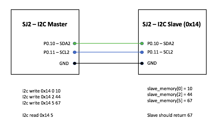
Part 0: Understand existing I2C Master driver
Gather per-requisite knowledge:
- I2C Bookstack page
- Read I2C chapter in your LPC User manual
- Scan the
i2c.handi2c.cfile, and understand the existing driver - Thorough understanding of pointers
Unless you have read the material above minimum of 5-10 times, there is no point moving forward into this lab. It is extremely important that you are familiar with the I2C bus before you dive into this lab. You should then understand the existing I2C driver that you will be "extending" to support slave operation. Start with the header file interface, and correlate that to the other reading material mentioned above.
Part 1: Attempt to read and write existing devices
Part 1.a: Setup
- Load sample project, reboot, and take a note of the I2C discovered devices on startup
- There is a boot message indicating various different addresses of the existing I2C slaves
- Turn on debug printfs at
i2c.c, re-compile, and re-load the modified project to the board- This will let you trace through I2C states as a read or write transaction is happening
- Look for
#define I2C__ENABLE_DEBUGGINGand set this to non-zero
Part 1.b: Read and Write Slave memory
Next step is to get familiar with the I2C CLI command and the existing I2C master driver, which allows you to read and write an I2C Slave devices' memory.
- Load the sample project
- Try the
i2c readandi2c writeCLI commands and attempt to read data from a device, such as the acceleration sensor.- This sensor is at address
0x38 - Open up
MMA8452Q.pdfand read theWHO_AM_Iregister - Write the
CTRL_REG1register and activate the sensor - Attempt to read X and the Z-axis and observe that the Z-axis should output the effect of gravity
- This sensor is at address
- Pause here, and go through the output debug printfs and cross check them against the I2C Master state machine diagram
Part 2: Draw your I2C Slave State Machine
Your objective is to act like an I2C slave device. Just like the acceleration sensor, you will act like a slave device with your own memory locations that a Master device can read or write. The first step in doing so is to draw your I2C Slave driver state machine that you will implement in your code.
Build the following table for your I2C Slave states:
| HW State | Why you got here? | Action to take |
The key to making the table above is:
- Understanding the I2C Master driver
- For each HW state of the Master driver, there is a corresponding Slave state
- Table 512 - 515 in the LPC User Manual
Part 3: Implement your I2C Slave driver
Part 3.a
In this step, we will configure your Slave board to respond to a particular I2C bus address. We will add minimal code necessary to be able to be recognized by another master.
Believe it or not, you only have to write a single function to be recognized as a slave on the I2C bus. Since the I2C Master driver is already initialized, you already have the setup for the Pin FUNC, and the I2C clock, so merely setting up the slave address recognition is needed. Locate the I2C registers and configure your Slave Address registers.
Pause here, and attempt to reboot the I2C Master board, and it should recognize your Slave address on startup. Do not proceed further until you can confirm that your slave address setup is working.
// TODO: Create i2c_slave_init.h
void i2c2__slave_init(uint8_t slave_address_to_respond_to);Notice that on the I2C slave board, it will print an entry to a new (un-handled) state each time the master board reboots and tries to "discover" the slave devices.
Hint
- The I2C
DATregister is only valid prior to clearing the SI bit- Clear the SI bit AFTER you read the
DATregister
- Clear the SI bit AFTER you read the
- I2C
ADDRandMASKregister- MASK can be set to non-zero to allow multiple address recognition
-
For example, if MASK is
0xC0and ADDR is0xF0, then your slave will recognize the following addresses:0x30,0x70,0xB0, and0xF0because MASK bit7 and bit6 indicate that those will not be "matched"
Part 3.b
In this step, you will do the following:
- Add extra states to the I2C Interrupt Handler that are relevant to your I2C slave driver
- Invoke callbacks which will interface your virtual I2C device
// TODO: Create a file i2c_slave_functions.h and include this at the existing i2c.c file
/**
* Use memory_index and read the data to *memory pointer
* return true if everything is well
*/
bool i2c_slave_callback__read_memory(uint8_t memory_index, uint8_t *memory);
/**
* Use memory_index to write memory_value
* return true if this write operation was valid
*/
bool i2c_slave_callback__write_memory(uint8_t memory_index, uint8_t memory_value);
// TODO: You can write the implementation of these functions in your main.c (i2c_slave_functionc.c is optional)The functions you added above should be called by your i2c.c state machine handler when the right state has been encountered. This should directly be related to your Part 2.
Inside the interrupt, you may have to save data variables as the interrupt cycles through the I2C states. The best way to handle this is to add more data members to typedef i2c_s; after which you can access members of this struct inside the I2C ISR.
Part 3.c
In this step, we provide the skeleton code that you need to integrate in your main.c at your Slave board.
#include "i2c_slave_functions.h
#include "i2c_slave_init.h"
static volatile uint8_t slave_memory[256];
bool i2c_slave_callback__read_memory(uint8_t memory_index, uint8_t *memory) {
// TODO: Read the data from slave_memory[memory_index] to *memory pointer
// TODO: return true if all is well (memory index is within bounds)
}
bool i2c_slave_callback__write_memory(uint8_t memory_index, uint8_t memory_value) {
// TODO: Write the memory_value at slave_memory[memory_index]
// TODO: return true if memory_index is within bounds
}
int main(void) {
i2c__init_slave(0x86);
/**
* Note: When another Master interacts with us, it will invoke the I2C interrupt
*. which will then invoke our i2c_slave_callbacks_*() from above
* And thus, we only need to react to the changes of memory
*/
while (1) {
if (slave_memory[0] == 0) {
turn_on_an_led(); // TODO
} else {
turn_off_an_led(); // TODO
}
// of course, your slave should be more creative than a simple LED on/off
}
return -1;
}Final Requirements
I2C State Machine Lab Submission:
- For part 1 (Attempt to read and write existing devices) - Serial terminal screenshots of memory being read and written.
- Logic analyzer screenshots for WHO_I_AM, CTRL_REG1 and for reading Accelerometer XYZ axis data.
- For Part 2 - Design I2C slave state machine for Master Write and Slave Read, Master Read and Slave Write along with the table of I2C slave state in both cases.
I2C Lab:
- Complete Part 3 - Attach Screenshots if you have any.
- Extra Credit for Creative Slave device and Multi-byte read/write.
- Creative Slave device - Your slave device should act like a real device and do things based on the setting of its slave memory registers
- Your slave should be able to read and write multiple registers in a single I2C transaction.
I2C communication on the same board
An alternative to test the I2C Leader-member (master-slave) communication on the same board is to make one of the i2c port(I2C2) as Leader(Master) and any of the available ports (I2C0/I2C1) as member (Slave).
Steps:
- Create
i2c_slave_init.h and i2c_slave_init.cfiles. Define a functioni2c_slave_init(...)which assigns slave address and slave configuration for a given i2c port. (Refer i2c__initialize function in i2c.c) - Also refer
peripherals_init.cto get more info on how I2C2 is initialized. - Call the
i2c_slave_init(...)function in your main.c - Connect the SDA and SCL pins of I2C2 with the respective SDA and SCL pins of I2C0/1
- Flash the code and try issuing
i2c detectcommand to see if you see a response from member device
You will still need to check a couple of things (CLK, IOPIN registers) before the driver becomes fully functional.
Lesson Watch Dogs
Watchdogs
Watchdog is a timer which can continuously check if there is any malfunction in the system operation and perform certain actions to restore normal operation. Watchdogs are commonly found in embedded system devices and provides self reliance to the system. It can take timely action to a critical failure in the system thereby restoring the system to a safe state.

Operation of a standard watchdog timer
There are hardware and software watchdogs. Hardware watchdog awaits a signal/pulse from a resource in the system during its timer period. If it receives the signal, it will reset itself and restart the timer. This continues till the system operations are normal and stable. If the resource fails or there is any fault in the system, the watchdog receives no indication during its timer period. Once the timer period elapses, it can take certain actions to bring the system back to stable state. The action could be resetting the system or any other action which restores normal operation.
Software watchdog is a task which monitors other tasks. Each task will report to the watchdog about its normal operation. If any of the tasks misbehave, then the watchdog can alert the user/system or take corrective action to get the task back to normal state.
Task Resuming & Suspending
A freeRTOS task that is currently running can be suspended by another task or by its own task. A suspended task will not get any processing time from the micro-controller. Once suspended, it can only be resumed by another task.
API which can suspend a single task is:
void vTaskSuspend( TaskHandle_t xTaskToSuspend );Refer this link to explore more details on the API. https://www.freertos.org/a00130.html
API to suspend the scheduler is:
void vTaskSuspendAll( void );Refer this link to explore more details on the API. https://www.freertos.org/a00134.html
void vTaskResume( TaskHandle_t xTaskToResume );Refer this link to explore more details. https://www.freertos.org/a00131.html
BaseType_t xTaskResumeAll( void );Refer this link to explore more details. https://www.freertos.org/a00135.html
EventGroups
Event group APIs can be used to monitor a set of tasks. A software watchdog in an embedded system can make use of event groups for a group of tasks and notify/alert the user if any of the task misbehaves.
Each task uses an event bit. After every successful iteration of the task, the bit can be set by the task to mark completion. The event bits are then checked in the watchdog task to see if all the tasks are running successfully. If any of the bits are not set, then watchdog task can alert about the task to the user.
Below are the APIs that can be used. Refer to each of the API to understand how to use them in your application.
- xEventGroupCreate
- xEventGroupCreateStatic
- xEventGroupWaitBits
- xEventGroupSetBits
- xEventGroupSetBitsFromISR
- xEventGroupClearBits
- xEventGroupClearBitsFromISR
- xEventGroupGetBits
- xEventGroupGetBitsFromISR
- xEventGroupSync
- vEventGroupDelete
Lab Assignment: Watchdogs
Objective
- Learn File I/O API to read and write data to the SD card
- This requires a micro SD card that is formatted with FAT32
- Design a simple application that communicates over the RTOS queue
- Implement a "Software" Watchdog through FreeRTOS EventGroups API
Prerequisite Knowledge
File I/O
You will be using a "file system" API to read (or write) a file. This is a third-party library and is not part of the standard C library, and it is connected to the SD card using the SPI bus.
Please read this page for API details; here is the overall data flow which allows you to use high-level API to read and write a file.
Watchdog
- A "watchdog timer" is a hardware timer
- It can count up or count down based on the implementation
- The objective is that when it reaches a ceiling, then it will trigger CPU reset
void main(void) {
watchdog_enable(100ms);
while (true) {
pacemaker_logic();
// If this function does not run within 100ms, the CPU will reset
watchdog_checkin();
}
}
Lab
Part 0: Setup Producer and Consumer Task
- Create a
producer taskthat reads a sensor value every 1ms.- The sensor can be any input type, such as a light sensor, or an acceleration sensor
- After collecting 100 samples (after 100ms), compute the average
- Write average value every 100ms (avg. of 100 samples) to the
sensor queue - Use medium priority for this task
- Create a
consumer taskthat pulls the data off thesensor queue- Use infinite timeout value during
xQueueReceiveAPI - Open a file (i.e.: sensor.txt), and append the data to an output file on the SD card
- Save the data in this format:
sprintf("%i, %i\n",time, light)" - Note that you can get the time using
xTaskGetTickCount()- The sensor type is your choice (such as light or acceleration)
- Note that if you write and close a file every 100ms, it may be very inefficient, so try to come up with a better method such that the file is only written once a second or so...
- Also, note that periodically you may have to "flush" the file (or close it) otherwise data on the SD card may be cached and the file may not get written
- Use medium priority for this task
- Use infinite timeout value during
Note:
- By configuration, fatfs only support FAT32. Thus, any MicroSD larger than 32 GB needs to be reformatted to FAT32.
- Alternatively, you can modify the
ffconfig.hto enable exFAT support.
#include "ff.h"
#include <string.h>
// Sample code to write a file to the SD Card
void write_file_using_fatfs_pi(void) {
const char *filename = "file.txt";
FIL file; // File handle
UINT bytes_written = 0;
FRESULT result = f_open(&file, filename, (FA_WRITE | FA_CREATE_ALWAYS));
if (FR_OK == result) {
char string[64];
sprintf(string, "Value,%i\n", 123);
if (FR_OK == f_write(&file, string, strlen(string), &bytes_written)) {
} else {
printf("ERROR: Failed to write data to file\n");
}
f_close(&file);
} else {
printf("ERROR: Failed to open: %s\n", filename);
}
}
Part 1: Use FreeRTOS EventGroup API
What you are designing is a software check-in system and thus emulating a "Software Watchdog".
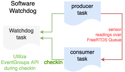
- At the end of the loop of each task, set a bit using FreeRTOS event group API.
- At the end of each loop of the tasks, set a bit using the
xEventGroupSetBits() -
producer taskshould set bit1,consumer taskshould set bit2 etc. - You are expected to read about the FreeRTOS Event Group API yourself
- At the end of each loop of the tasks, set a bit using the
- Create a
watchdog taskthat monitors the operation of the two tasks.- Use high priority for this task.
- Use a task delay of 1 second, and wait for all the bits to set. If there are two tasks, wait for bit1, and bit2 etc.
- If you fail to detect the bits are set, that means that the other tasks did not reach the end of the loop.
- Print a message when the Watchdog task is able to verify the check-in of other tasks
- Print an error message clearly indicating which task failed to check-in with the RTOS Event Groups API
void producer_task(void *params) {
while(1) { // Assume 100ms loop - vTaskDelay(100)
// Sample code:
// 1. get_sensor_value()
// 2. xQueueSend(&handle, &sensor_value, 0);
// 3. xEventGroupSetBits(checkin)
// 4. vTaskDelay(100)
}
}
void consumer_task(void *params) {
while(1) { // Assume 100ms loop
// No need to use vTaskDelay() because the consumer will consume as fast as production rate
// because we should block on xQueueReceive(&handle, &item, portMAX_DELAY);
// Sample code:
// 1. xQueueReceive(&handle, &sensor_value, portMAX_DELAY); // Wait forever for an item
// 2. xEventGroupSetBits(checkin)
}
}
void watchdog_task(void *params) {
while(1) {
// ...
// vTaskDelay(200);
// We either should vTaskDelay, but for better robustness, we should
// block on xEventGroupWaitBits() for slightly more than 100ms because
// of the expected production rate of the producer() task and its check-in
if (xEventGroupWaitBits(...)) { // TODO
// TODO
}
}
}
Part 2: Thoroughly test the Application
-
Create a CLI to "suspend" and "resume" a task by name.
- "task suspend task1" should suspend a task named "task1"
- "task resume task2" should suspend a task named "task2"
- Run the system, and under normal operation, you will see a file being saved with sensor data values.
- Collect the data over several seconds, and then verify by inserting the micro-SD card to your computer
- Plot the file data in Excel to demonstrate.
- Suspend the
producer task- The watchdog task should display a message and save relevant info to the SD card.
- Observe the CPU utilization while your file is being saved
- You should observe that the SD card task should utilize more CPU
What you created is a "software watchdog". This means that in an event when a task is stuck, or a task is frozen, you can save relevant information such that you can debug at a later time.
You may use any built-in libraries for this lab assignment such as a sensor API
Conclusion
What to turn in
- Positive test case scenario with serial terminal indicating tasks are running normally
- Suspension of a task, and then negative test case scenario with serial terminal indicating which task failed to check-in
- Data plot as mentioned in Part 2
- All relevant source code (compiled and tested)
FreeRTOS Trace
Please use TraceAlyzer to open this trace and inspect what is going on. The company offers "Academic License" to view the attached file (click on the link above).
Lesson X
Executable Format and Boot Loader
JTAG
C vs. C++
Typically, C design pattern to create a re-usable module is performed like so:
typedef struct {
int target_ms;
int interval_ms;
} timer_t;
void timer_start(timer_t *t, uint32_t interval);
void timer_stop(timer_t *t);
bool timer_expired(timer_t *t);On the other hand, C++ for the same module would be:
class timer
{
public:
void start(uint32_t interval);
void stop();
bool expired();
private:
int target_ms;
int interval_ms;
};Code analysis
void main(void)
{
/**
* C convention:
* object_method(&obj)
* Then you pass the object as the first parameter to the methods to "operate on" this object
*/
timer_t t;
timer_start(&t, 1000);
timer_stop (&t);
/**
* C++ convention:
* obj.method()
*
* C++ automatically passes the object pointer, known as the "this" pointer to the method
* In reality, the language and the compiler is invoking the methods just like C:
* timer::start(&obj, 1000);
*/
timer t;
t.start(1000);
t.stop();
}Volatile Variable

// volatile
int flag; // global memory is part of "BSS" section, guaranteed to be zero (unless a bug in startup code)
void flag_setter_task(void *p) {
while (1) {
++flag;
vTaskDelay(1000);
}
}
void flag_checker_task(void *p) {
puts("Task entry");
while (1) {
flag = 0;
while (0 == flag) {
;
}
puts("flag has incremented away from value of 0");
vTaskDelay(1000);
}
}
Interview Questions
- What is a
volatilekeyword? - Given a code snippet, why you cannot set a breakpoint?
- Is
constopposite of volatile? - What is the point of "
const volatile *variable" ?- You as a programmer, cannot write a line of code to modify, but maybe DMA or a peripheral behind you can modify it
Random Topics
Useful topics to learn about:
- Avoid dynamic memory after RTOS starts
- Avoiding task deletions
- APIs to avoid in FreeRTOS
- How much sleep time will vTaskDelay(1) actually sleep the task?
- Clock system review
- Peripheral clock divider
- CPU PLL
FreeRTOS X
Critical Section
Objective
To go over Critical Sections in an application as well as other kernel API calls that, which for the most part, you should refrain from using unless necessary.
What are Critical Sections
Critical sections (also called critical regions) are sections of code that makes sure that only one thread is accessing resource or section of memory at a time. In a way, you are making the critical code atomic in a sense that another task or thread will only run after you exit the critical section.
Implementations of a critical section are varied. Many systems create critical sections using semaphores, but that is not the only way to produce a critical section.
How to Define a Critical Section
/* Enter the critical section. In this example, this function is itself called
from within a critical section, so entering this critical section will result
in a nesting depth of 2. */
taskENTER_CRITICAL();
/* Perform the action that is being protected by the critical section here. */
/* Exit the critical section. In this example, this function is itself called
from a critical section, so this call to taskEXIT_CRITICAL() will decrement the
nesting count by one, but not result in interrupts becoming enabled. */
taskEXIT_CRITICAL();Code Block 1. Entering and Exiting a Critical Section (FreeRTOS.org)
Using the two API calls taskENTER_CRITICAL() and taskEXIT_CRITICAL(), one is able to enter and exit a critical section.
Implementation in FreeRTOS
Typically, when FreeRTOS is ported to a system, critical sections will STOP/DISABLE the OS Tick interrupt that calls the RTOS kernel. If the OS tick interrupt triggers during your critical section, the interrupt is in a pending state until you re-enable interrupts. It is not missed, but is delayed due to the interrupts that get disabled.
If you task takes too long to do its operation, RTOS can perform in a real time manner because it has been shutdown during your critical section. Which is why you need to super selective about using a critical section.
The FreeRTOS implementation for Critical Sections by Espressive (ESP32 platform) does not use RTOS, but actually uses a mutex that is passed in instead. It becomes an abstraction to using semaphore take and give API calls.
Critical Section with interrupt enable/disable vs. Mutex
First of all, a mutex provides you the ability to guard critical section of code that you do not want to run in multiple tasks at the same time. For instance, you do not want SPI bus to be used simultaneously in multiple tasks. Choose a mutex whenever possible, but note that a critical section with interrupt disable and re-enable method is typically faster. If all you need to do is read or write to a few standard number data types atomically then a critical section can be utilized. But a better alternative would be to evaluate the structure of your tasks and see if there is really a need to use a mutex or critical section.
Use a mutex when using a peripheral that you must not use simultaneously, like SPI, UART, I2C etc. For example, disabling and re-enabling interrupts to guard your SPI from being accessed by another task is a poor choice. This is because during the entire SPI transaction, you will have your interrupts disabled and no other (higher) priority tasks can get scheduled and the OS could miss its ticks. In this case, a mutex is a better choice because you only want to guard the tasks from accessing this critical section from each other, and you do not need care if other tasks get scheduled if they will not use the SPI bus.
FreeRTOS Producer Consumer Tasks
Objective
- Learn how Tasks and Queues work
- Assess how task priorities affect the RTOS Queue cooperative scheduling
Queues and Task Priorities
Tasks of equal priority that are both ready to run are scheduled by the RTOS in a round-robin fashion. This type of context switch is called Preemptive Context Switch.
Queues' API can also perform context switches, but this is a type of Cooperative Context Switch. What this means is that if xQueueSend() API is sending an item to a higher priority task that was waiting on the same queue using the xQueueReceive() API, then the sending task will switch context inside of the xQueueSend() function over to the other task. Therefore, task priorities matter when using the queue API.
Also note that when the cooperative context switch occurs, it does not wait for the next tick of preemptive scheduling to switch context. Typical RTOSes support both cooperative and preemptive scheduling, and in fact, you can turn off preemptive scheduling in FreeRTOSConfig.h
static QueueHandle_t switch_queue;
typedef enum {
switch__off,
switch__on
} switch_e;
// TODO: Create this task at PRIORITY_LOW
void producer(void *p) {
while (1) {
// This xQueueSend() will internally switch context to "consumer" task because it is higher priority than this "producer" task
// Then, when the consumer task sleeps, we will resume out of xQueueSend()and go over to the next line
// TODO: Get some input value from your board
const switch_e switch_value = get_switch_input_from_switch0();
// TODO: Print a message before xQueueSend()
// Note: Use printf() and not fprintf(stderr, ...) because stderr is a polling printf
xQueueSend(switch_queue, &switch_value, 0);
// TODO: Print a message after xQueueSend()
vTaskDelay(1000);
}
}
// TODO: Create this task at PRIORITY_HIGH
void consumer(void *p) {
switch_e switch_value;
while (1) {
// TODO: Print a message before xQueueReceive()
xQueueReceive(switch_queue, &switch_value, portMAX_DELAY);
// TODO: Print a message after xQueueReceive()
}
}
void main(void) {
// TODO: Create your tasks
xTaskCreate(producer, ...);
xTaskCreate(consumer, ...);
// TODO Queue handle is not valid until you create it
switch_queue = xQueueCreate(<depth>, sizeof(switch_e)); // Choose depth of item being our enum (1 should be okay for this example)
vTaskStartScheduler();
}
Assignment
- Finish
producer taskthat reads a switch value and sends it to the queue- Create an enumeration such as
typedef enum { switch__off, switch__on} switch_e;
- Create an enumeration such as
- Create a queue, and have the
producer tasksend switch values every second to the queue - Finish
consumer taskthat is waiting on the enumeration sent by theproducer task
After ensuring that the producer task is sending values to the consumer task, do the following:
- Ensure that the following is already setup:
- Print a message
producer taskbefore and after sending the switch value to the queue - Print a message in the
consumer taskbefore and after receiving an item from the queue - You may use the following:
printf("%s(), line %d, sending message\n", __FUNCTION__, __LINE__);
- Print a message
Note down the Observations by doing the following:
- Use higher priority for
producer task, and note down the order of the print-outs - Use higher priority for
consumer task, and note down the order of the print-outs - Use same priority level for both tasks, and note down the order of the print-outs
Answer Additional Questions:
- What is the purpose of the block time during
xQueueReceive()? - What if you use ZERO block time during
xQueueReceive()?
What to turn in
- Submit all relevant source code
- Relevant screenshots of serial terminal output
- Submit explanation to the questions as comments in your code at the top of your source code file
- Explanation of the Observations
- Explanation for the Additional Questions
Extra Credit
This extra credit will help you in future labs, so it is highly recommended that you achieve this. You will add a CLI handler to be able to:
- Suspend a task by name
- Resume a task by name
Please follow this article to add your CLI command. Here is reference code for your CLI:
app_cli_status_e cli__task_control(app_cli__argument_t argument, sl_string_t user_input_minus_command_name,
app_cli__print_string_function cli_output) {
sl_string_t s = user_input_minus_command_name;
// If the user types 'taskcontrol suspend led0' then we need to suspend a task with the name of 'led0'
// In this case, the user_input_minus_command_name will be set to 'suspend led0' with the command-name removed
if (sl_string__begins_with_ignore_case(s, "suspend")) {
// TODO: Use sl_string API to remove the first word, such that variable 's' will equal to 'led0'
// TODO: Or you can do this: char name[16]; sl_string__scanf("%*s %16s", name);
// Now try to query the tasks with the name 'led0'
TaskHandle_t task_handle = xTaskGetHandle(s);
if (NULL == task_handle) {
// note: we cannot use 'sl_string__printf("Failed to find %s", s);' because that would print existing string onto itself
sl_string__insert_at(s, "Could not find a task with name:");
cli_output(NULL, s);
} else {
// TODO: Use vTaskSuspend()
}
} else if (sl_string__begins_with_ignore_case(s, "resume")) {
// TODO
} else {
cli_output(NULL, "Did you mean to say suspend or resume?\n");
}
return APP_CLI_STATUS__SUCCESS;
}